
Last Updated on March 16, 2024
Designing Regulator circuit with low dropout regulation and high output current is quite complex process. But Diodes Incorporated provides ready made solution by AZ1117E. Here we have designed 1.0A Low Dropout Linear Regulator circuit by using AZ1117E.
The AZ1117E is a low dropout three-terminal regulator with 1.0A
output current ability, and the dropout voltage is specified at typical
1.1V at 1.0A current load, decreasing at lower load currents. The AZ1117E has been optimized for low voltage where transient response and minimum input voltage are critical. It provides current limit and thermal shutdown protection. This IC has on chip thermal protection setup to avoid high current ambient temperature.
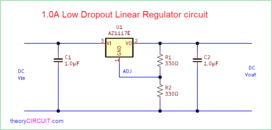
Circuit Diagram of Adjustable Regulator
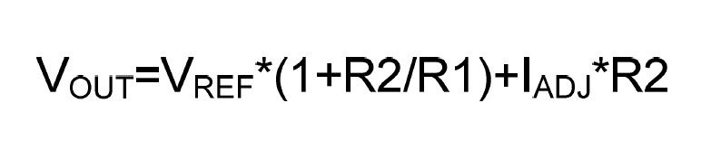
Output Voltage Calculation
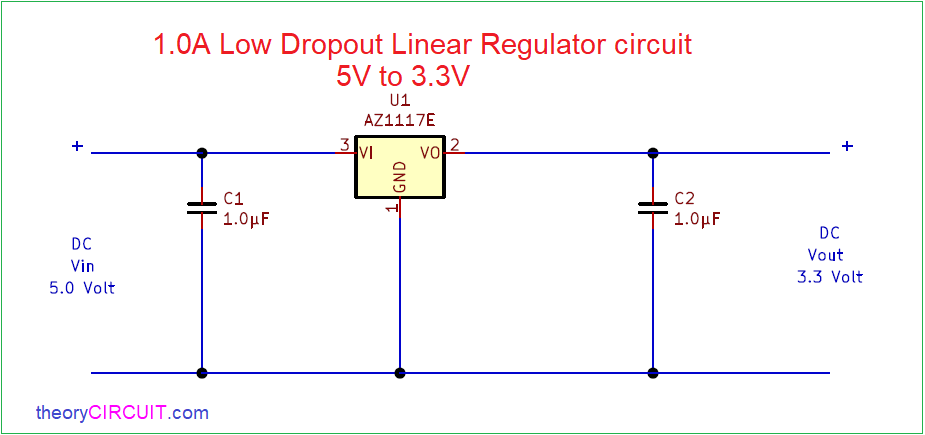
Circuit Diagram of Fixed Regulator
Components Required
- IC AZ1117E
- Capacitor 1.0µF = 2 SMD 0805
- Resistor 330Ω = 2 SMD 0805
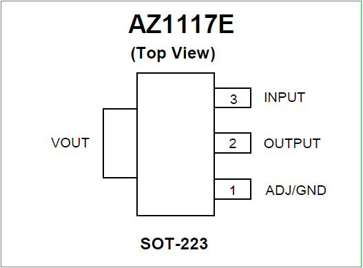
AZ1117E Pin details
The AZ1117E is available in 1.2V, 1.5V, 1.8V, 2.5V, 3.3V and 5.0V
fixed output voltage versions and ADJ output voltage version. The
fixed versions integrate the adjust resistors. This IC available in SOT-223 package. It has three terminal Named as pin 1 ADJ/GND, pin 2 OUTPUT and pin 3 INPUT. It will provide good load regulation at 1A current output. It can take upto 16 volt as input and Gives 1.5 Volt to 12 Volt as output.
For Adjustable voltage regulator design using AZ1117E we need to put voltage divider setup at output using two Resistors. Here we have used R1 and R2 Resistors and connected ADJ pin between the voltage divider Resisters. Output voltage is depends on the value of these two Resistors (R1 and R2). Capacitors C1 and C2 works as voltage filters.
For fixed voltage regulator design using AZ1117E we need to choose fixed output voltage range IC (1.2V, 1.5V, 1.8V, 2.5V, 3.3V and 5.0V ). This circuit will require only filter capacitors at input and output. We have used two 1.0µF ceramic capacitors.