Last Updated on March 16, 2024
Simple 9V Audio Power Amplifier Circuit using LM4755 designed with few External Resistors and Capacitors. As we know Designing Stereo audio power amplifier always requires lot of external element and cost also increases depends on the count of components. On other hand by looking at specific, special and application oriented Audio Amplifier ICs we can reduce designing cost. Here Stereo Audio power amplifier circuit designed by using LM4755 IC from Texas Instruments and it delivers 11 Watt output per channel to 4Ω Loud speaker or 7W per channel into 8Ω using a single 24V supply. Due to the Internal mute circuit and pre set gain resistors we don’t need to put more external components.
Before jumping in to the Amplifier circuit design, let us know about the basic details of IC LM4755.
LM4755
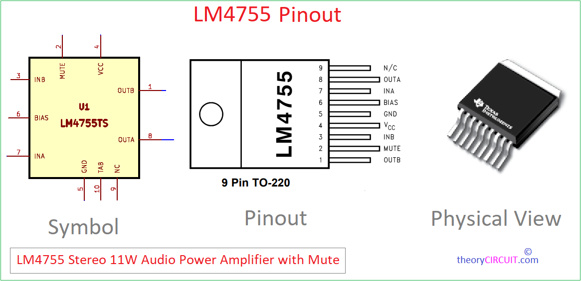
Symbol of LM4755 should be in Typical Amplifier shape, here I just showed schematic symbol, This IC Drives 4Ω and 8Ω Loud speakers (Output Watts may vary), This IC operates in Single and dual power supply. Accepts Operating Voltage Range between 9V to 40V. It have internal gain resistors setup, Internal Current Limiting and Thermal protection. It gives Closed Loop Gain 34 dB and Output Power at 10% THD with 1kHz into 4Ω at VCC = 24V 11 W. Using 9V supply will reduce the output power. LM4755 comes in Compact 9-lead TO-220 Package and 9 Pin DDPAK Package, hence it is easy to deploy on PCB board with heat pad. This IC most suitable for low component Stereo applications.
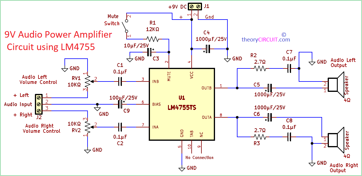
Circuit Diagram
Components Required (BOM)
| 1 | C1, C2, C7, C8 | 0.1μF | C_Disc_D3.0mm_W1.6mm_P2.50mm | 4 | ||
| 2 | C4, C5, C6 | 1000μF/25V | CP_Radial_D12.5mm_P5.00mm | 3 | ||
| 3 | C3 | 10μF/25V | CP_Radial_D8.0mm_P5.00mm | 1 | ||
| 4 | C9 | 100μF/25V | CP_Radial_D8.0mm_P5.00mm | 1 | ||
| 5 | R2, R3 | 2.7Ω | R_Axial_DIN0309_L9.0mm_D3.2mm_P12.70mm_Horizontal | 2 | ||
| 6 | R1 | 12KΩ | R_Axial_DIN0309_L9.0mm_D3.2mm_P12.70mm_Horizontal | 1 | ||
| 7 | U1 | LM4755TS | TO97P1435X457-10N | 1 | ||
| 8 | LS1, LS2 | Speaker | PinHeader_1x02_P2.54mm_Vertical | 2 | ||
| 9 | RV1, RV2 | 10KΩ | Potentiometer_Alps_RK09K_Single_Horizontal | 2 | ||
| 10 | Switch | Mute | SW_DIP_SPSTx01_Slide_9.78×4.72mm_W7.62mm_P2.54mm | 1 | ||
| 11 | J1 | 9V DC | TerminalBlock_Altech_AK300-2_P5.00mm | 1 | ||
| 12 | J2 | Audio Input | TerminalBlock_Altech_AK300-3_P5.00mm | 1 |
Construction & Working
Audio left and right inputs are connected with IC LM4755 input pins INB and INA through 10KΩ Variable resistors VR1, VR2 and Coupling capacitors C1, C2, these capacitors blocks unwanted DC voltages at the input of Amplifier and also eliminates high frequency noise. Mute pin 2 is connected to 9V DC supply through R1 and C3 capacitor, these elements provides mute function timing to LM4755. At the output side pin 1 delivers Audio left output to 4Ω speaker through output coupling capacitor C5 and pin 8 delivers Audio right output through coupling Capacitor C6. At both outputs R2, R3 & C7, C8 provides stabilization at the output stage from high frequency oscillations.
Once the circuit wiring is complete, provide stereo audio input at the designated terminals (J1) and observe the stereo output response through loud speakers. It’s crucial to note that the circuit’s output power can be influenced by the bias supply voltage (Vcc) and the speaker Coil resistance. To optimize the audio response, it’s advisable to employ a regulated power supply setup in this circuit. LM4755 acts as Class AB architecture audio amplifier and provides 83KΩ input impedance and also Provides 80dB mute attenuation in mute mode.
Connect the potentiometer as mentioned in the circuit, that is shaft left edge pin is to be connected to the GND and right edge to be connected to the Audio input signal, By the way rotating the shaft of the potentiometer, you can control the volume of the output audio signal to the loud speaker. When the wiper is closer to the input side, the volume will be Higher, and when it’s closer to the ground side, the volume will be Lower.
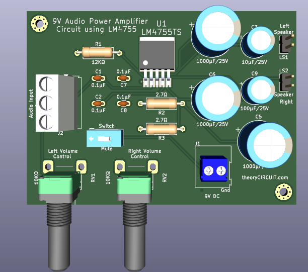
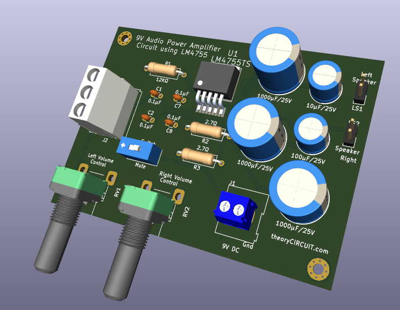
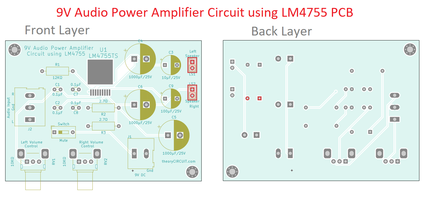
Printed Circuit Board
9V Audio Power Amplifier Circuit using LM4755 PCB Gerber Files.
Interactive Board Viewer


9V Audio Power Amplifier Circuit using LM4755 PCB View