Last Updated on March 16, 2024
Circuit which converts Frequency of input signal into a proportional Voltage output is known as Frequency to Voltage converters some times it termed as FVCs or F to V Converters. Frequency measurement is required in numerous applications like Liquid flow measurement, Tachometers and speed control, Light Intensity Measurement, Vibration Monitoring and Temperature measurement etc.., Here Frequency to Voltage Converter Circuit using 555 Timer designed to implement in such projects and applications.
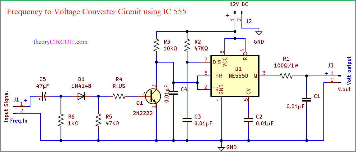
Here IC 555 configured in Monostable Multivibrator mode and it produce output pulse depends on the input frequency level. Before this stage input signal frequency is converted into triggering spike signal by using Capacitor C5 and Diode D1. This triggering spike should be equal to 2/3 or 1/3 of VCC applied to the timer IC 555.
Circuit Diagram
Components Required For PCB (BOM)
| 1 | C1, C2, C3, C4 | 0.01μF | C_Disc_D3.4mm_W2.1mm_P2.50mm | 4 | ||
| 2 | C5 | 47μF | CP_Radial_D5.0mm_P2.00mm | 1 | ||
| 3 | R2, R5 | 47KΩ | R_Axial_DIN0207_L6.3mm_D2.5mm_P10.16mm_Horizontal | 2 | ||
| 4 | R1 | 100Ω/1W | R_Axial_DIN0309_L9.0mm_D3.2mm_P12.70mm_Horizontal | 1 | ||
| 5 | R3 | 10KΩ | R_Axial_DIN0207_L6.3mm_D2.5mm_P10.16mm_Horizontal | 1 | ||
| 6 | R4 | 10Ω | R_Axial_DIN0207_L6.3mm_D2.5mm_P10.16mm_Horizontal | 1 | ||
| 7 | R6 | 1KΩ | R_Axial_DIN0207_L6.3mm_D2.5mm_P10.16mm_Horizontal | 1 | ||
| 8 | D1 | 1N4148 | D_DO-35_SOD27_P7.62mm_Horizontal | 1 | ||
| 9 | U1 | NE555D | DIP-8_W7.62mm | 1 | ||
| 10 | Q1 | 2N2222 | TO-92 | 1 | ||
| 11 | J1 | I/P Signal | PinHeader_1x02_P2.00mm_Vertical | 1 | ||
| 12 | J2 | 12V DC | PinHeader_1x02_P2.00mm_Vertical | 1 | ||
| 13 | J3 | V.out | PinHeader_1x02_P2.00mm_Vertical | 1 |
Construction & Working
Input signal either Square wave or Sine wave should be converted into triggering spike before reaching timer IC triggering pin then only we can oscillate mono pulse depends on the triggering signal. Output pulse duration is depends on the Timing Resistor R3 and Timing Capacitor C4. Output from the timer IC is connected to the Output pin headers J3 through R1 and C1. Here C1 Removes noise spike in output pulse (Voltage). Transistor Q1 is connected across the Timing Capacitor C4, Input signal is converted into triggering spike by using C5 and D1 elements and reaches base terminal of Q1. When the positive potential rises Q1 gets turn ON and Discharges C4 Capacitor. When the Negative potential rises Q1 gets turn OFF and gives time to C4 for charging. This cycle repeats depends on the input signal frequency.
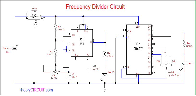
By this way timer IC frequently triggered by input signal frequency and gives output Pulse (Potential difference – Voltage). Calibrate this circuit and tune components value depends on your need. If you are looking for a circuit which divides the input frequency and gives output. Following Schematic will help you.
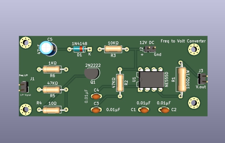
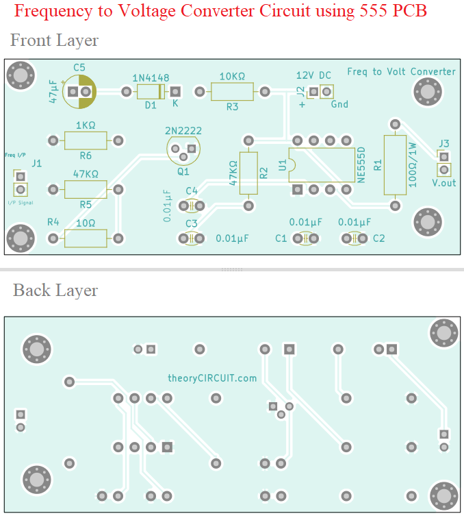
Printed Circuit Board
Frequency to Voltage Converter Circuit using 555 Gerber Files.
Interactive Board Viewer


Frequency to Voltage Converter Circuit using 555 PCB