
Last Updated on March 16, 2024
To protect sensitive electronic or electric load we need protection circuits such as over voltage protection circuit, over current protection circuit, reverse supply protection circuit or surge protection circuit. By implementing these circuit we can ensure the protection of sensitive load. Here Crowbar Overvoltage Protection Module circuit is designed to protect a bulb load.
We know Crowbar Overvoltage Protection Module is a over voltage protection circuit and by applying the voltage regulator zener diode we can set the output voltage limit to this crowbar circuit. For an example here we taken a 12V DC bulb and applied different voltage and tested the crowbar circuit with over voltage beyond 12 volt.
Circuit Diagram
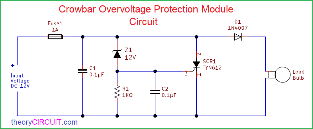
Components Required
- Glass fuse 1A
- Zener diode 12V
- SCR TYN612
- Capacitor 0.1µF = 2
- Resistor 1KΩ
- Diode 1N4007
- 12V DC bulb
Construction & Working
This crowbar over voltage protection circuit is designed to cut the power supply to sensitive load when over voltage flows. This prototype uses a 12V bulb as sensitive load hence we need to design crowbar circuit for 12V and so the 12V zener diode regulator place in this circuit. First start with the glass fuse and place the thyristor SCR TYN612 across the load and apply gate supply through zener diode. Here diode 1N4007 is used to protect reverse voltage.
By using variable power supply unit we have applied the power supply to this circuit and by applying voltage below 12V and upto 12V the load gets power supply and when we apply input supply beyond 12V then SCR gets gate supply through zener diode and makes the short circuit through Anode and Cathode pins and so the fuse blown hence the over voltage don’t reach the sensitive load.
SCR TYN612 Pin diagram
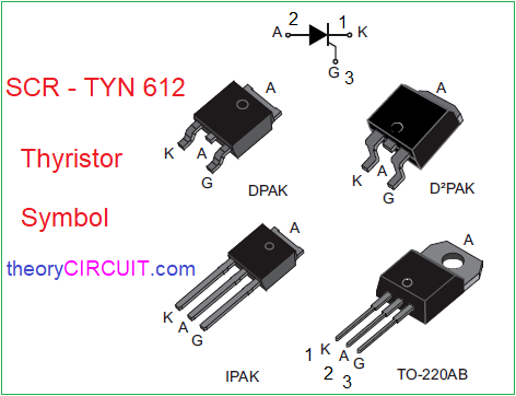
SCR TYN612 comes in different packages and it has three pins called Anode (A), Cathode (K) and Gate (G). It can be used in current limiting or voltage regulation and rectification circuits.