Last Updated on March 31, 2024
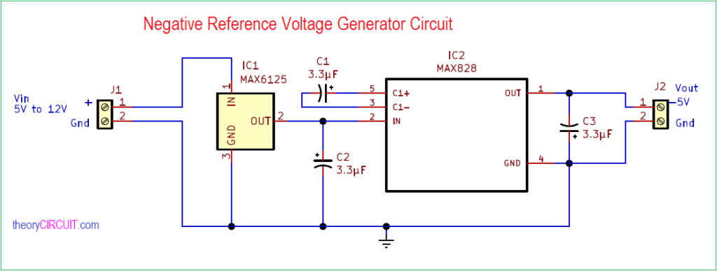
Negative Reference Voltage Generator Circuit designed by using simple charge-pump inverter and a positive output voltage reference. In this circuit design we don’t use external Resistors or negative voltage source. We can use this negative reference voltage generator at tiny space and low power circuit design.
This circuit employs MAX6125 ( Low-Dropout, 3-Terminal Voltage References ) and MAX828 ( Switched-Capacitor Voltage Inverter ) from maxim. This circuit requires only three external capacitor for its full operation.
Circuit Diagram
Components Required
| J1 | Screw_Terminal_01x02 | TerminalBlock:TerminalBlock_Altech_AK300-2_P5.00mm |
| J2 | Screw_Terminal_01x02 | TerminalBlock:TerminalBlock_Altech_AK300-2_P5.00mm |
| IC1 | MAX6125 | Package_TO_SOT_SMD:SOT-23 |
| IC2 | MAX828 | Package_TO_SOT_SMD:SOT-23-5 |
| C1 | 3.3µF | Capacitor_SMD:C_0805_2012Metric |
| C2 | 3.3µF | Capacitor_SMD:C_0805_2012Metric |
| C3 | 3.3µF | Capacitor_SMD:C_0805_2012Metric |
Construction & Working
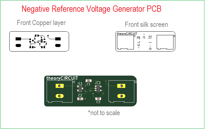
Use Negative Reference Voltage Generator Gerber files for PCB, Assemble SMD components as mentioned in the schematic. There is no inductor and variable resistors hence this circuit elements occupies very little space. The first IC gives voltage reference to the switched capacitor inverter IC2 from Vin. Depends on the input power supply the IC2 delivers up to -5 V as negative reference voltage.
PCB
Negative Reference Voltage Generator PCB Gerber.
Interactive Board Viewer


