Last Updated on October 28, 2024
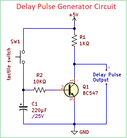
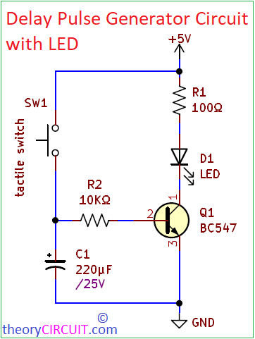
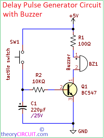
Delay Pulse Generator Circuit have a lot of hidden applications, that can be used in any time delay or timing action required projects. Technically it is a single shot timing circuit build by using single stage transistor and timing Capacitor & Resistor. This circuit is build by few commonly available components. It can be easily modified to give long or short duration delay pulse at the output. Here we have tested this circuit with LED and Buzzer.
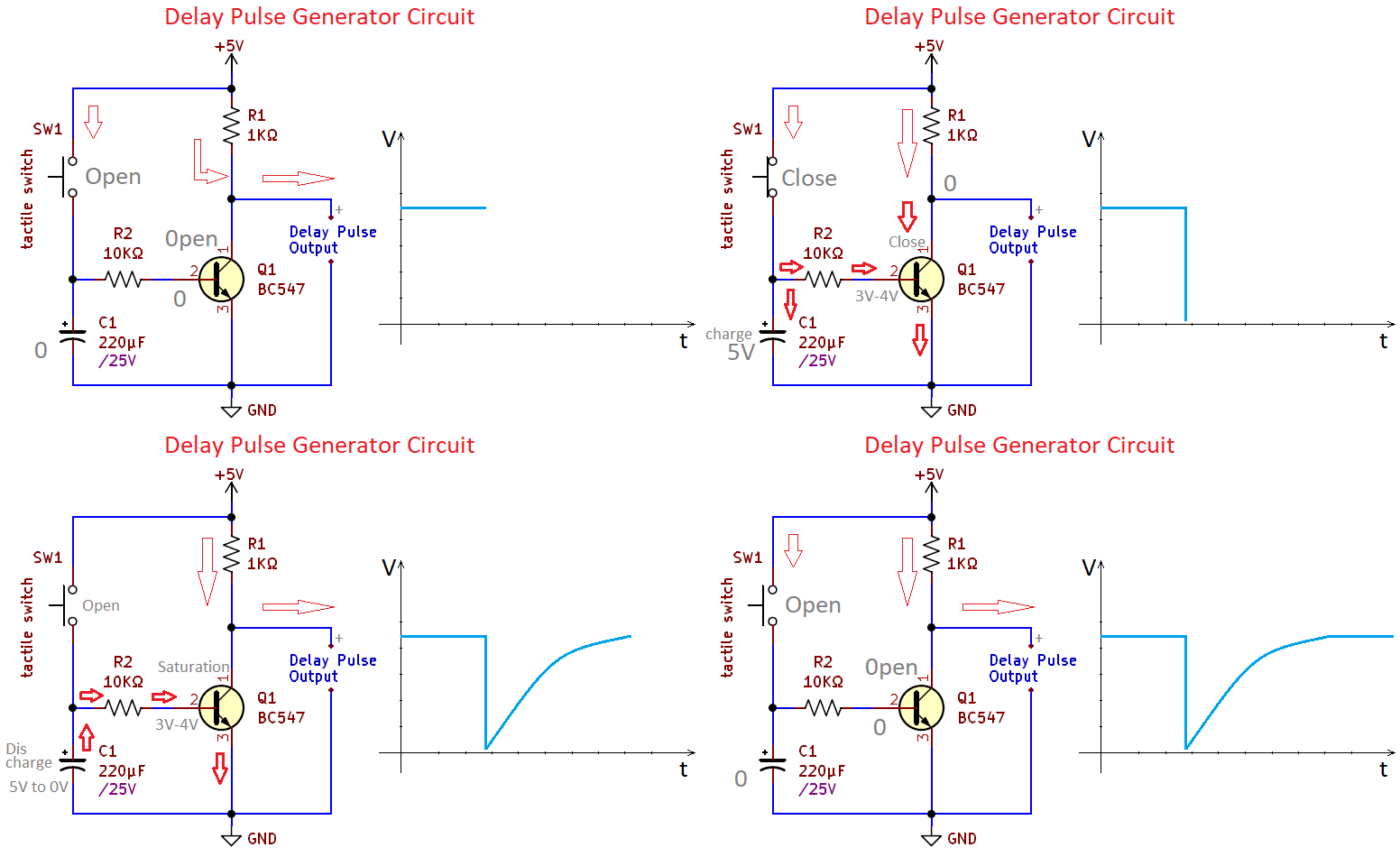
This single stage delay pulse generator circuit have a RC Network formed by R2 (10KΩ) and C1 (220μF), this network decides the time delay at the output.
Circuit Diagram
Components Required
- Transistor BC547 NPN (Q1)
- Capacitor 220µF/25V (C1)
- Resistor 10KΩ (R2)
- Resistor (R1) 1KΩ (Taking pulse output), 100Ω (for LED or Buzzer)
- Tactile Switch (SW1)
- 5V DC supply
Working Video
Construction & Working
Here we using NPN Transistor BC547 as a Switch you can use any NPN transistor which have (0.7V) base threshold voltage for turn ON operation. After completing the circuit connection, when we press the switch SW1 (tactile switch press and release), +V supply flows to the Capacitor C1 and makes it charging, and also gradually increase the voltage at the base of Transistor Q1 through R2 Resistor. When this voltage reaches the threshold level (0.7V), then the transistor gets turn ON and makes pulse.
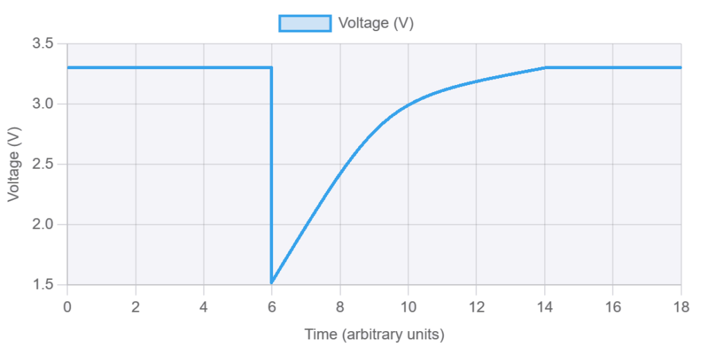
Here we take output from collector terminal side so the voltage level drops to zero from +Vcc and then slowly recovers to +Vcc as the capacitor discharge gradually.
Initial State (Switch Off)
When we turn ON the circuit, SW1 in open condition, so the Capacitor C1 have no charge so the voltage to Q1 base terminal is zero. So the Transistor Q1 remains OFF. Hence output between collector terminal and GND will be high as +V (Vcc) supply.
SW1 Press & Release
When the SW1 switch pressed & Released, the Capacitor C1 will get direct +V supply (Another terminal of C1 is already connected to GND) and so it gets charged. This charge is flows to the base terminal of Q1 through R2 (10KΩ) Resistor, it is the only way for Capacitor to discharge. It makes transistor Q1 turn ON. Hence the output between collector to GND becomes low to GND or 0.
Time Delay
It is depends on the Capacitor discharge time through R (timing resistor, here R2). It can be written as,
Time = Rt * Ct
Time = R2 * C1
Time = 10000Ω * 0.00022F
Time = 2.2 Seconds (approximately)
It is extended or shorted by the characteristics of Transistor and Capacitor.

