Last Updated on July 22, 2024
A Circuit used to increase the voltage output is known as voltage booster circuit, it can called as voltage step up circuit. Here we use DC input and get DC output so that it can be termed as DC-DC Voltage boost converter circuit. It is used where load requires high voltage than Input or applied DC supply. Basic operation of this circuit is depends on the storage element and switching components. Here we designed simple voltage booster circuit using transistor with Inductor.
Most booster circuit use Inductor (L) as a storage element, and it stores energy in the form of magnetic flux when the current flows through it and release it when the current flow is interrupted. To make this operation continuous without stopping we can use any switching components (BJT, MOSFET) with timing control and by varying the switching speed we can get desired high DC Voltage than input DC.
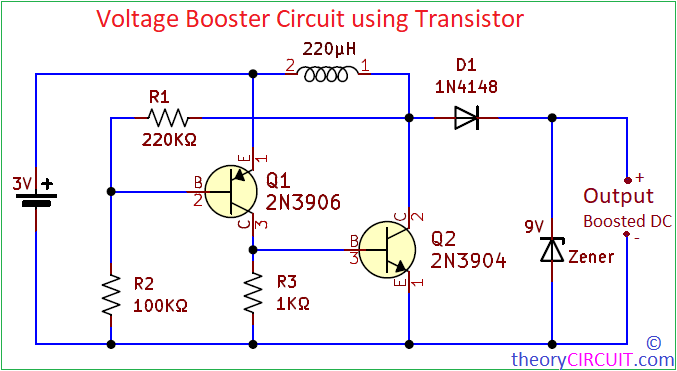
Circuit Diagram
Components Required
- Transistor PNP 2N3906
- Transistor NPN 2N3904
- Inductor 220µH
- Diode 1N4148
- Zener Diode 9V
- Resistor 220KΩ, 100KΩ, 1KΩ = each one
- Battery 3V
- Connecting wires
Simulation Output
LTspice Simulation of Voltage Booster circuit using two transistor as switch and one Inductor as charging element.
Construction & Working
In this transistor switch and inductor based booster circuit 3V DC given as Input and boosted 9V DC obtained as output. Transistor Q1 base is connected to the Inductor, (Q2) collector junction through R1, and base terminal of Q2 is connected to the collector terminal of Q1. This setup creates feedback switching circuit. Diode D1 used to rectify the high voltage spikes from Inductor and the Zener diode regulates the output DC. Connecting filter capacitor with proper voltage rating at the output before Zener diode is recommended for filtering DC.
When the power supply is ON current flow occurs through Inductor to output terminal so it gets magnetized (charging) slowly during initial time then it gets fully charged and reach Q1 transistor base and makes it turn ON by the way Q2 also gets base supply and turn ON, then the whole charge from Inductor rapidly discharged. Then two transistor comes to OFF condition without any base supply from inductor. Again the Inductor gets charge and this cycle repeats. This rapid charge and discharge makes high voltage spikes and it is rectified by the diode D1, hence we receive high DC output voltage.

