Last Updated on January 12, 2025
Logic Gates are essential elements in digital circuit. For to perform logical operations on binary inputs & digital signals, we need logic gates. If we need custom logic gate in a Embedded System or Circuits, we spent lot of time to find perfect IC (speaking about standalone device design). But often we forgot that we can design logic gates using Transistors, for our own specifications. Here we are going to make experiment to design logic gates using BC547 NPN Transistor (easily available component) and test it with truth table.
Transistor BC547 have three terminals called Collector (C), Base (B) and Emitter (E). When the VBE (Base to Emitter) Voltage reaches 0.7V, then the Transistor gets ‘ON’ (saturated region) and allows current to flow between the Collector to Emitter terminal. If the VBE gets down below 0.7V or GND then the Transistor goes to ‘OFF’ state (cut off region), these characters makes transistor as a switch, and we are going to use this character to design logic gates.
Here we used +5V as bias to the Transistor and logic input 1 (HIGH) as +5V and logic input 0 (LOW) as GND. In the base terminal we used 10KΩ Resistor to drop the voltage, and it will enough to drive the transistor. We have designed logic gates NOT, AND, OR, NAND, NOR & XOR gates using transistor and used LED to show +the logic output. If the LED glows, it represents Logic HIGH and if the LED off, it represents logic LOW.
Components Required
- Transistor BC547 (NPN) = 3
- LED = 1
- Resistors 10KΩ = 2, 1K = 1
- Breadboard
- Connecting wires
- power supply (DC 5V)
Working Video
NOT Gate
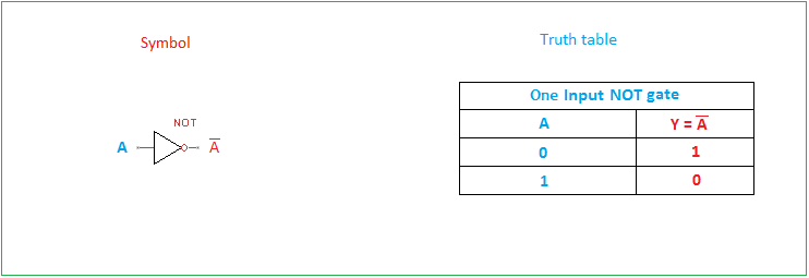
A Logic NOT gate Inverts the input. Gives Logic HIGH for LOW input and Changes output to LOW if we apply Logic HIGH input. It will have only one input and one output terminal.
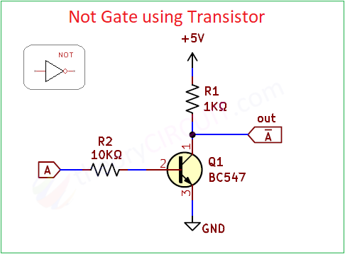
This single transistor acts as NOT gate and takes input A and gives A’ (inverted) output. You can use any general purpose or switching transistor for to make logic gates. When the input (A) is low (0V or GND) then the transistor BC547 remains in off condition so the output is pulled high (5V) by the resistor R1 and giving a logic HIGH output. When the input is high (5V) then the transistor turns on by getting enough VBE and creating a path to ground through its collector-emitter junction. This pulls the output to 0V (logic LOW). Hence this circuit inverts the input signal, if the input is 0, the output is 1, and if the input is 1, the output is 0.
AND Gate
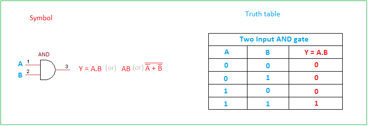
A logic AND gate gives HIGH output only when the all inputs are HIGH and gives LOW output for other inputs.
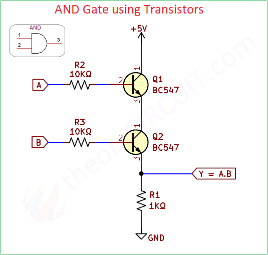
Connect two Transistors in series and take output from the Q2 transistor emitter and R1 Resistor junction, Base terminals of Q1, Q2 acts as input terminals. When both inputs A and B are LOW (0V or GND) both transistors Q1 or Q2 will be in off state. So there is no path to +5V reach the Q2 emitter and R1 junction, So the output will be LOW (GND). If only one of the inputs is HIGH, either Q1 or Q2 will turn ON, but not both. Due to series connection, there is no path to +5V to reach the Q2 emitter and R1 junction, So the output will be LOW (GND). When both inputs A and B are high, both Q1 and Q2 transistors gets turn ON and makes path to +5V to reach the Q2 emitter and R1 junction, So the output pulled to +5V that is Logic HIGH (1). Hence this circuit gives output HIGH only when both inputs are HIGH, which matches the behavior of an AND gate.
OR Gate
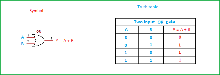
A logic OR gate gives LOW output only when the all inputs are LOW and gives HIGH output for other inputs.
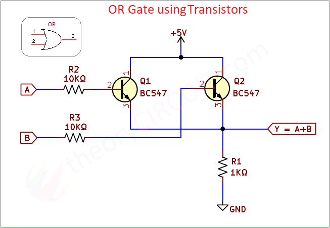
Connect both transistor (Q1, Q2) in parallel and take output from the emitter and R1 Resistor junction. Base terminal of Q1, Q2 acts as input A, B. When both inputs A and B are low (0V or GND) then the transistors Q1, Q2 will be in OFF state. As a result, there is no path to +5V to reach the emitter and R1 Resistor Junction, so the output Y remains low (0V or GND), which is logic LOW. If either input A or B is high (5V) then the corresponding transistor (Q1 or Q2) will get turns on and makes a path to +5V to reach the emitter and R1 Resistor junction. This pulls the output Y to HIGH (5V),that is logic HIGH output. If both inputs are HIGH then then the output will be HIGH as stated previously, because Q1, Q2 are connected in parallel. This behavior resembles logic OR gate character.
NAND Gate
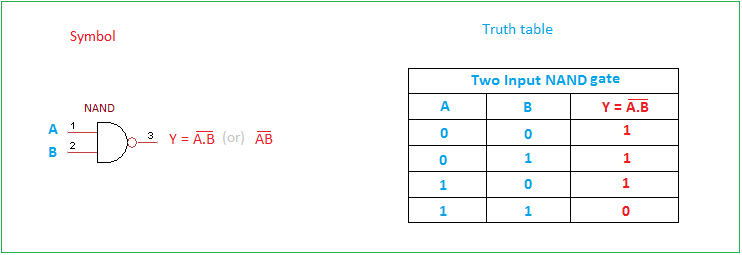
A logic NAND gate gives LOW output only when all inputs are HIGH and gives logic HIGH output for remaining combinations of inputs.
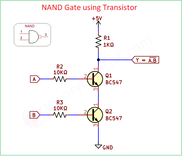
Connect two transistors (Q1, Q2) in series and take output from R1 Resistor and Q1 Collector terminal junction (R1, Q1 Junction). Two transistor Q1, Q2 base terminals will acts as inputs A, B. When both inputs are HIGH then the transistors Q1, Q2 gets turn ON and makes path to +5V to reach GND, so there will be no bias at the R1,Q1 Junction, this will result output as LOW (0 or GND). If any one input or both inputs are LOW (0) then the transistor either Q1,Q2 or both will be in off state. So there will be no path to +5V to reach GND and the output from R1, Q1 Junction remains HIGH (+5V).
NOR Gate
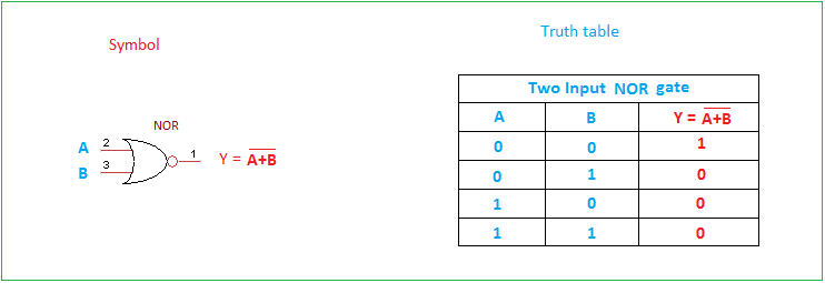
A logic NOR gate gives HIGH output only when all inputs are LOW and gives logic LOW output for remaining combinations of inputs.
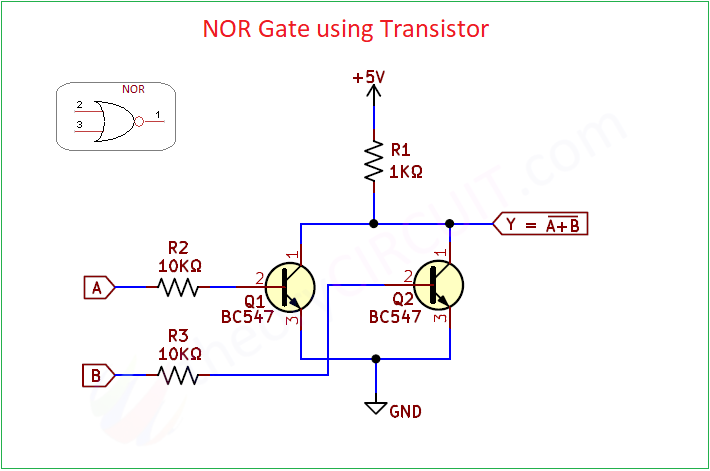
Connect two transistors (Q1, Q2) in parallel and take output from R1 Resistor, Collector Junction, base terminal of Q1, Q2 acts as input A, B. When both inputs are LOW (0 or GND) then the transistor Q1, Q2 stays in off condition, so there is no path to +5V reach GND and the output from the R1 Resistor, Collector junction pulls the +5V as output that is Logic HIGH. If any one transistor gets logic HIGH input, then there will be path to +5V to reach GND and the output will be LOW.
XOR Gate
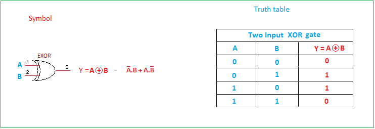
An XOR (exclusive OR) gate gives output as HIGH (1) only when it receives the different inputs like 0, 1 or 1, 0. If the both inputs are same, either HIGH (1) or LOW (0) then the XOR gate output will be LOW (0).
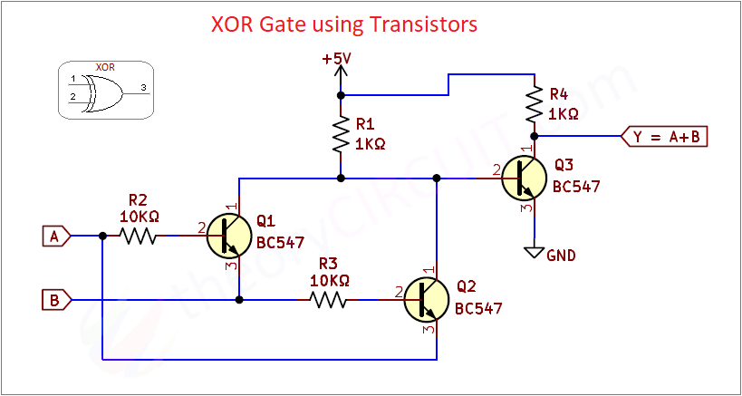
Logic XOR gate designed by using three BC547 transistors (Q1, Q2, and Q3). The input A is connected to the base of Q1 through resistor R2 (10KΩ), and the input B is connected to the base of Q2 through resistor R3 (10KΩ). The collector of Q1 and Q2 connected to the +5V bias through R1 (1KΩ) resistor and also this junction is connected to the base terminal of Q3 transistor. The emitter of Q1 is connected to the base of Q2 through R3 (10KΩ) resistor, and the emitter of Q2 is connected to the base of Q1 through R2 (10KΩ) resistor and these two transistors makes a cascading connection between them. The collector of Q3 is connected to +5V via pull up resistor R4 (1KΩ) and the emitter terminal is grounded. The output Y (A⊕B) is taken from the collector of Q3 and R4 resistor junction. This configuration ensures the desired XOR operation by controlling the conduction of Q3 based on the states of Q1 and Q2 transistors.

I like the work and i will be happy if more interesting circuits and videos /exsplanations be given me.