
Last Updated on March 16, 2024
In Electronics R&D, prototyping and Hobby a Waveshpe plays important role that is Square Wave, to generate it we use timer ICs, Transistors. When we are thought to get a Square pulse output, instantly IC 555 Astable Multivibrator circuit will popup in our mind. Offcourse 555 timer rocks but that has some limitations like Only one output, Minimum operating Voltage start from +5V, Temperature tollarance is 0°C to 70°C. If you want to generate Square pulse for Digital Electronics circuits, Microcontrollers, Clock signal input, Frequency Testing, Frequency multiplication and division and for Time delay applications. You can give a try to the following “Square Wave Pulse Generator Circuit using IC CD4047”.
About IC CD4047
CD4047 is a CMOS Low Power Monostable/ Astable Multivibrator, this IC is Manufactured by various semiconductor companies, the CD4047 serves a dual purpose, functioning both as a monostable vibrator (single Shot) and an Astable oscillator. In monostable mode, the IC generates a single pulse in response to an external trigger, making it valuable in applications like pulse shaping and time delay circuits. When configured as an Astable multivibrator, it becomes an excellent square wave generator, essential for clock circuits, digital communication, and frequency-controlled devices.
CD4047 Pinout
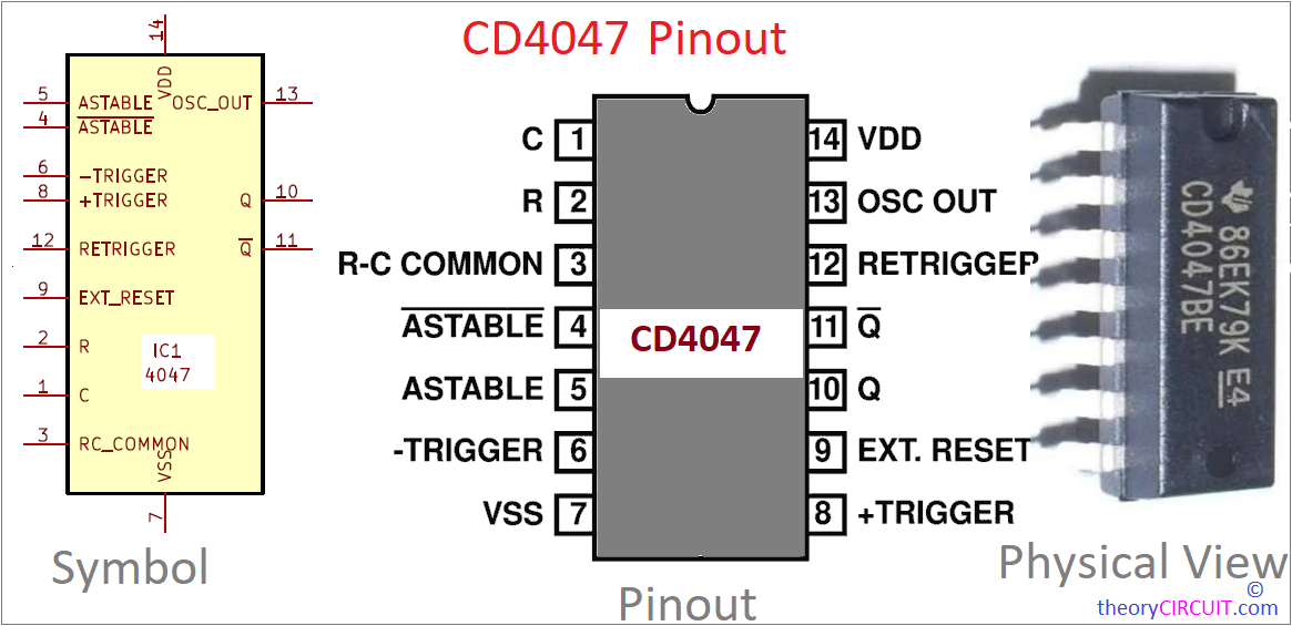
Pin Configuration of IC CD4047
| Pin No. & Pin Name | Pin Description |
| 1, C | External Timing Capacitor |
| 2, R | External Timing Resistor |
| 3, R-C COMMON | Common pin for Timing Resistor and Capacitor junction. |
| 4, {~ASTABLE} ACTIVE LOW | Making it LOW (GND) makes CD4047 as Astable Multivibrator |
| 5, ASTABLE | Making it HIGH (VDD) makes CD4047 as Astable Multivibrator |
| 6, – TRIGGER | High to Low Transition input during Monostable Multivibrator Mode |
| 7, VSS | Ground supply Pin |
| 8, + TRIGGER | Low to High Transition input during Monostable Multivibrator Mode |
| 9, EXT.RESET | External Reset Pin, Makes Output Q to LOW and Q’ (Q bar) to HIGH |
| 10, Q | Output Pin |
| 11, {~Q} Q BAR | Inverted Output Pin |
| 12, RETRIGGER | Retrigger pin allows the IC to respond to successive trigger pulses, extending the output pulse duration in monostable mode. |
| 13, OSC OUT | Oscillated Output pin |
| 14, VDD | Positive Supply Pin |
This IC CD4047 is operates with wide Voltage range from 3V to 15V and consumes very low power due to its CMOS design., It can give uninterrupted output even in temperature range from -55°C to 125°C. It gives Output Q and Inverted Output Q bar. For monostable mode it have two different triggering method and allows multiple triggering.
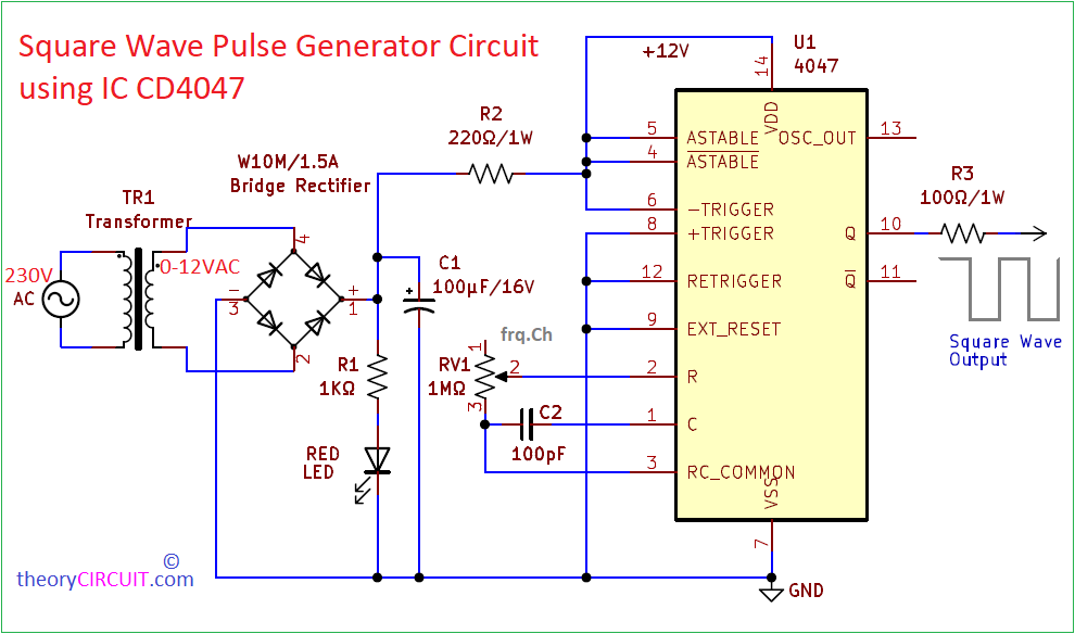
Circuit Diagram
Components List
- Stepdown Transformer 230V to 12V AC/1 Amps
- Bridge Rectifier Module W10M
- CD4047 IC Astable/Monostable Multivibrator
- Resistor 1KΩ, 220Ω, 100Ω each one
- Variable Resistor 1MΩ
- LED Red 5mm
- Capacitor 100μF, 100pF each one
Construction & Working
Construction of This Square Wave Pulse Generator Circuit using IC CD4047 starts from Stepdown Transformer and Bridge Rectifier module W10M, which converts 12V AC supply in 12V DC supply, due to wide operating Voltage range of CD4047, we are not using Voltage Regulator setup here, if you want you can introduce 12V Zener diode at the Rectifier Output after filter capacitor C1. Here LED indicates the presence of powersupply.
To Configure CD4047 in Astable Mode (Continuous Pulse Generation), we have to give HIGH (VDD) to Pin 5,4,and 6 (Astable, Astable’ bar, and – Trigger) and then LOW (GND) to Pin 8, 9, 12 (+ Trigger, Ext_Reset, Retrigger). Now the IC comes in Astable mode, for timing oscillation this IC Requires only two components that is Resistor and Capacitor. A Variable Resistor 1MΩ is connected with pin 2 and Capacitor 100pF is connected with pin 1 and the junction point of R and C is connected with pin 3. Finally output pulse is obtained from pin 10 (Q), you can get inverted output from pin 11 (Q bar). Here you can Vary the pulse frequency but you can not vary the duty cycle. This IC always gives 50% duty cycle at the output. Output frequency of this IC can be calculated by the following formula.
F = 1/8.8*R*C
For an Example,
F = 1/8.8RC, F = 1/(8.8*400KΩ*100pF), F = 1/(8.8*400000*0.0000000001), F = 1/(0.000352), F = 2840.90909 Hz, F = 2.841 KHz.
Output Frequency at the pin 13 can be calculated as, F = 1/(4.4 * R * C).