
Last Updated on April 15, 2024
If we need DC power supply for circuits we choose stepdown transformer based Rectifier circuit, It may give constant DC voltage under Regulator ICs but when the current fluctuations occurs at Input Power Source then the DC output supply will also gets affected.
We know that linear power supplies or stepdown transformer based power supply requires heavy transformers to step down the AC supply and then Rectifiers, Regulators to make it constant DC supply. Depends on the output current delivery, size of transformer increase. On the other hand, Switched Mode Power Supplies that is SMPS are compact in size and efficient devices used to convert Input AC Supply ranging from from 90 to 250 V (typical Value) to Desired level of DC Supply like 5V, 12V, 24V and -V etc., Here SMPS uses a controlled high frequency switching circuit to control the Output DC Supply. This enables SMPS to give desired output Voltage and Current.
To get rid of this drawback in traditional DC power supply method engineers, electronic designers are go with SMPS circuit. You may heard the name SMPS (Switched Mode Power Supply), It gives good constant DC output with considerably constant output current.
Switched Mode Power Supply design given in the form of simple SMPS Circuit diagram, We know SMPS is an essential device for modern electronics, to provide efficient power supply from AC to DC. A Typical SMPS circuit contains Various components like Transistors, Diodes, Capacitors, Inductors and Special Pulse Transformer, those are should meet with the requirement specifications and arranged in a feedback loop to regulate Voltage and Current flow. This article will help you to understand the SMPS diagram with explanation from the schematic of SMPS to the Practical Implementation. Operation principle of TNY267 based SMPS ckt remains same for 12V or 5V SMPS Circuit. Due to high voltage handling and isolation problem, you have to carefully follow the connection diagram of SMPS given here while wiring it for an application.
This page contains a simple smps circuit which is capable of producing 12 volt DC with 1 Amps current rating, and this circuit contains few easily available components, it may help you to design your own smps for your electronics projects.
SMPS Block Diagram
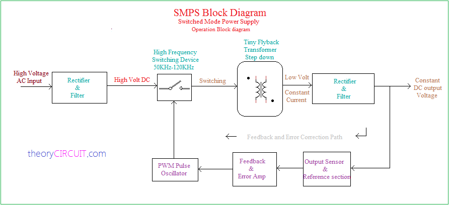
Before going to circuit diagram it is necessary to understand the operation of SMPS. This block diagram represents typical SMPS inner blocks.
We give high voltage AC Input and low frequency which is available on power outlet, the first stage of SMPS is Rectifier and filter hence the high AC becomes High Voltage DC from this operation we eliminate high spikes and surge, High voltage DC is controlled by High Frequency switching device (50KHz-120KHz) vary depends on design this switching block samples the high voltage DC with feed back path reference.
The flyback or tiny ferrite core transformer step down the voltage as required depends on design, then the second stage is Rectifier and filter section, it gives Rectified constant DC output Voltage without current fluctuations.
Some portion of output is taken as feedback signal and this signal compared with reference voltage and the error (if present) is amplified depends on the error PWM pulse changes its frequency hence the switching device regulates the output. So the minimum changes in output DC regulated instantly without affecting load.
Circuit diagram
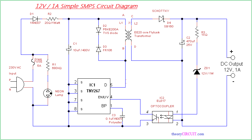
Construction & working
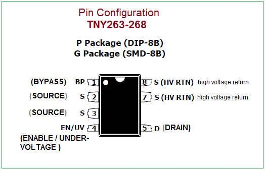
Main three parts of this simple SMPS circuit are TNY267 tiny switch -II family IC from power integrations. It is enhanced, energy efficient and low power offline switching device.
TNY 267 Pinout
Secondly EE20 core flyback transformer as stepdown transformer which is made up of compact ferrite EE. Middle column includes a cross-section of 4.5 x 4.5 mm, air gap 0.4 mm. Primary carries 157 turns of wire diameter 0.15 mm. Secondary incorporates (for 12V output) 14 turns of wire 0.4 mm.
Finally Optocoupler in feedback path IC2 EL817, it is a photo transistor opto coupler, when the output DC voltage goes beyond the limit then this optocoupler gives signal to TNY 267 IC, and then the PWM output pulse gets changers accordingly.
Use the components as specified and output will be 12V DC with 1 Amps current rating.
Note
1. This circuit Involves in operating High voltage AC it is lethal, Handle with extreme care
2. Make the Flyback transformer as your requirement or get a ready made one.
3. If you are construct your own Flyback transformer, then check the operation of the device before fetch into circuit.
4. Again, All stages in SMPS circuit involved in operation of High voltage either AC or DC, Handle with extreme care and protections.
Refer Datasheet for More Details.
For further Design and simulation, https://www.poweresim.com/ Free website dedicated for Switch Mode Power supply circuit “SMPS” Design and Transformer calculation web tool.
Could I get the PCB layout of this circuit?
Can I make a 2amp 5/12volt Smps using tny 267 Ic if possible then what is transformer and circuit design.
Thank you for the given information. My question is; can the current be increased more than 1Amp?. by connecting more copper wire in parallel or increase the thickness of the copper wire.
very good information Smps voltage circuit analysis. small question Smps PCB board tharmistor resisrot why this resistor use in smps.
to avoid heat , as it work on high frequency so the circuit will get heated,so to avoid this n keep circuit cool.
Thermistor is used as a circuit protection device, this component protect from short circuit and overload conditions, by preventing current flow to the rectifier section.
If an old ie transformer based supply uses a linear regulated output how does input power/voltage affect the output? If it’s designed correctly it doesn’t. The real reason smps’ are used is cost size and weight not regulation.
Hi There,
I am trying to find EE20 Core Flyback Transformer but unable to get it. Where can I get one any idea?
Hi Amit,
Try finding it in Alibaba website.
Thanks
Hi,
Could you please advise what type of transformer I should be using to get 5v output with more than 700mA current?
Thanks
Sir i had built this above circuit instead of using tny267 i had used tny266 because it was available to me and i had seen sam circuit diagram with that on this given blog rest all things are in common.
http://streampowers.blogspot.com/2015/08/12v-1a-smps-circuit-diagram.html?m=1
Now here is my problem i am not getting my required current out of it. It is not able to go beyond 450ma after that i think transformer is saturating and when i measure the output voltage it shows 13.8v in no load and 13.4 in small load is it normal?
Can i use it to output 110vdc
Could someone tell me how the transformer was wound, primary and secondary. Is the primary shielded from the secondary? what frequency? I have a similar circuit I’m working on but 325 dc rectified from 220ac. What does it mean if I keep blowing the pin 5 on the mosfet/tnyswitch. and many times R2 in your diagram.
I want to know what is the theory of transformer design.
THANK YOU.
pl. specify the input voltage does it works from 90v to 250v ac also I want to make 9V DC supply so I can use ZD1 9V/ 1Watt zener instead of 12 volts zener. Also the no of secondary turns 11 turns or 10turns.
Pl. help in this regard.
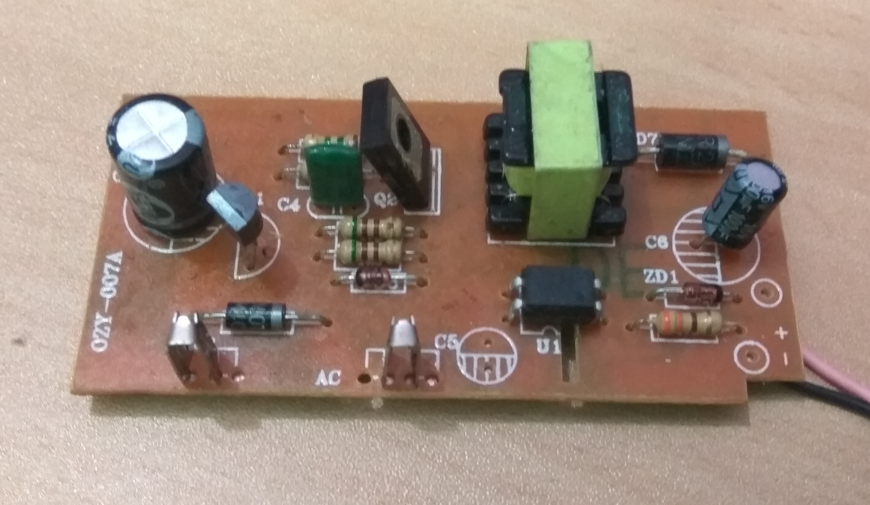
Dear Sirs… your SMPS Circuit Diagram and the PCB Board (in the Photograph) does not seem to match !
Q1 and Q2 are not given in the circuit. What values are Q1 & Q2 and how are they connected in the circuit ? or is the pcb photograph from a different circuit ? can you please clarify ?
Thanks in advance.
I m not getting 1amp output at load..
Good day Sir, is it possible to convert a portable mains Dell laptop charger to a DC type by replacing the AC input capacitor only.
Godfrey, NG.
Hi,
Do we have available flyback transformers on the market that can be used with the TNY267 circuit you provided since design a flyback is tough?
Sincerely,
Mike
This circuit fails to comply with any regulatory agency rules on EMI and RFI. Why doesn’t this circuit include an X2 safety capacitor and common mode choke? It should not be used without them as it would be illegal in most developed countries.
Hi Justin
This is Simple SMPS Circuit for who trying to built and understand switched mode power supply and not suitable for industrial or commercial applications.