Last Updated on March 16, 2024
TDA2003 is a monolithic audio power Amplifier integrated circuit. It requires very low external components to operated as a amplifier and also it can provide high current output. By implementing this TDA2003 IC in a low power audio amplifier we can built low harmonic and cross over distortion amplifier.
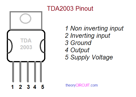
This IC has only 5 pins and all are function pins, this Integrated circuit has built in over temperature protection and short circuit protection features.
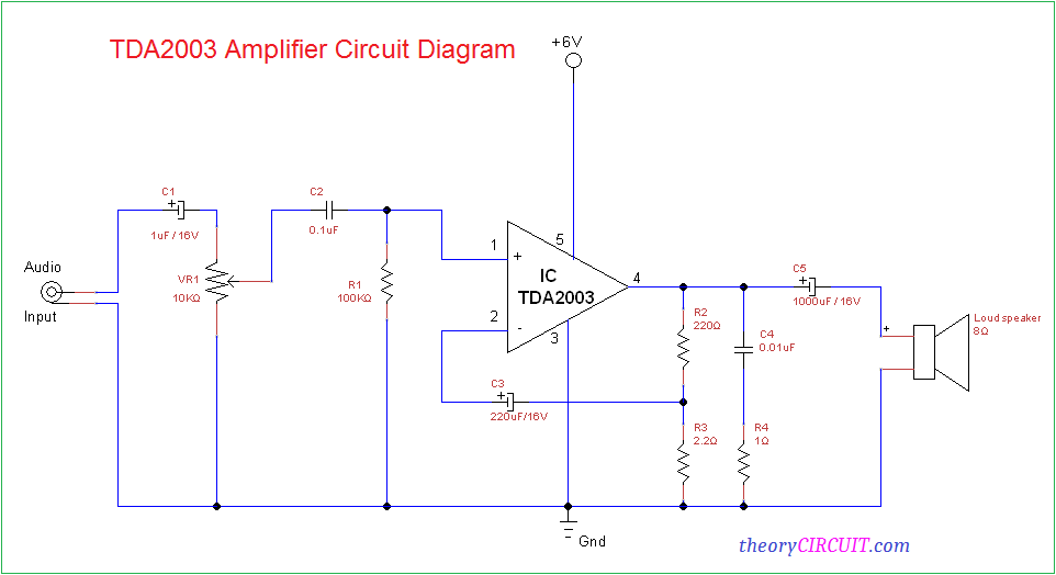
TDA2003 Amplifier circuit diagram built for 8Ω speaker and this circuit can provide upto 10 watts output, you can apply 6 to 12V power supply to this circuit.
Circuit Diagram
Construction & Working
Connect Audio input signal to non inverting pin of TDA2003 IC. Here VR1 is acts as a volume control in this circuit. Inverting pin of TDA2003 is connected with C3 capacitor and R2, R3 divider Resistors to act as a feedback path, at the output loud speaker is connected through coupling capacitor.
This TDA2003 amplifier can give upto 20 Watts output when connected in Bridge configuration.
TDA2003 Pinout
This TDA2003 IC can take supply voltage Vs between 8 to 18 Volts, and gives output power depends on load resistor RL, maximum 10 Watts if RL = 2Ω. It is sensitive to minimum 14 mV input signal and provides input resistance 150KΩ. Refer data sheet for more electrical specifications.
What about setting the gain?
Use VR1, R2 and R3.