
Last Updated on January 16, 2026
While working on signal testing and R&D activities on my work bench, I often felt need for a simple reliable signal amplifier that could quickly adapt to different testing conditions. Sometimes an Inverting output was required and sometimes Non Inverting output was required with adjustable gain, all without redesigning the whole circuit every time. This is where the idea for this circuit came from. Simple signal Amplifier with Gain control circuit using IC TL072.
I developed this as a utility circuit for signal analysis, debugging and experimentation, the goal was not to build a complex audio amplifier but to design compact and flexible to work with it and also that could sit on a test bench or to be dropped into an R&D setup whenever needed.
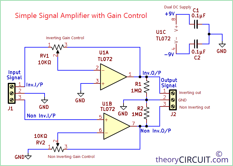
This circuit provides both Inverting and Non Inverting amplification each with independent gain control using a single IC TL072 dual op amp powered from a dual ±9V supply.
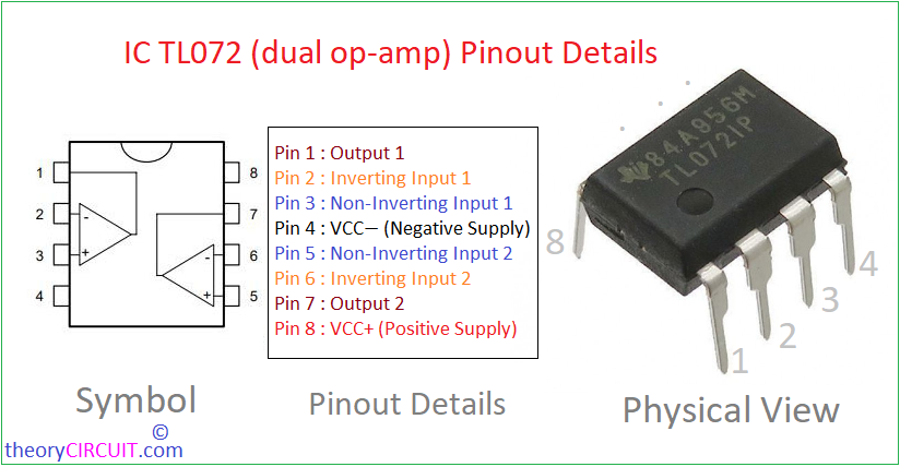
Why I Chose the TL072 Op-Amp IC?
The circuit needed to be stable, low noise and flexible across different gain variations without adding unwanted distortion or loading the signal source. So after considering several operation amplifier ICs I chose the TL072 for this circuit. One of the main reasons is its JFET Input stage, the TL072 has a very high input impedance, low noise performance, two matched op-amps in a single package and well suited for dual supply operation.
Circuit Diagram
Components Required
| 1 | C1, C2 | 0.1μF | C_Disc_D3.8mm_W2.6mm_P2.50mm | 2 | ||
| 2 | R1, R2 | 1MΩ | R_Axial_DIN0207_L6.3mm_D2.5mm_P10.16mm_Horizontal | 2 | ||
| 3 | U1 | TL072 | CERDIP-8_W7.62mm_SideBrazed_LongPads_Socket | 1 | ||
| 4 | RV1, RV2 | 10KΩ | Potentiometer_Piher_PT-6-V_Vertical_Hole | 2 | ||
| 5 | J1, J2, J3 | Screw_Terminal_01x03 | TerminalBlock_Altech_AK300-3_P5.00mm | 3 |
Working Simulation
Construction & Working
This circuit designed to have two sections one is Inverting Amplifier section (U1A) and another one is Non Inverting Amplifier section. Input signal is applied to dual Op-Amps through input connector J1 and output signal taken out from J2 connector.
This circuit can work with ±5V to ±15V dual DC supply, and the power lines are directly connected to the bias pins of IC TL072 that is +9V to pin 8 and -9V to pin 4 and then GND is the reference midpoint. Here i used C1, C2 (0.1μF) decoupling capacitors in the power pins.
Inverting Amplifier Section (U1A)
This first op-amp U1A is wired as a classic inverting amplifier with gain control element RV1 (10KΩ) here it is acts as a variable feedback Resistor, Output Gain here will be,
Gain (AV) = – (Rf/Rin)
So the output is 180° phase shifted.
Non Inverting Amplifier Section (U1B)
This second op-amp U1B is wired as a non-inverting amplifier with gain control element RV2 (10KΩ) here it is acts as a variable feedback Resistor and input signal directly applied to pin 5 (Non.Inv pin), Output Gain here will be,
Gain (Av) = 1 + (Rf/Rg)
here gain ≥ 1 and no phase inversion occurs.
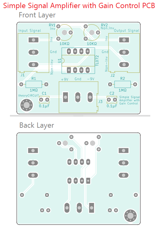
Printed Circuit Board
Simple Signal Amplifier with Gain Control Circuit Gerber Files.
Interactive Board Viewer


PCB 3D View
