
Last Updated on March 29, 2024
Voltage Doubler Circuit or Voltage Multiplier circuits are used to get higher DC Voltage than the Input AC Voltage. Basic operation of this circuit is to store and transfer energy from the input waveform to the output by using diodes and capacitors. Input of these circuit will be sinusoidal waveform or AC Voltage Source (Vs) and the output will be DC (Direct Current) supply. As the name says the output will be twice the maximum amplitude of input source signal.
Depends on the utilization (Rectification) of input wave we can classify Voltage doubler into two types.
- Half Wave Voltage Doubler
- Full Wave Voltage Doubler
you may heard of cockcroft walton voltage multiplier, that is comes under full wave voltage doubler type. In this article we are going to experiment half and full wave types.
Components Required
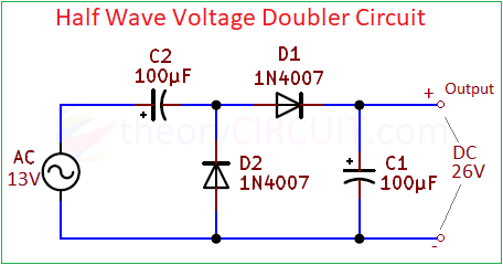
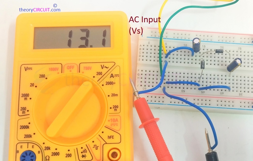
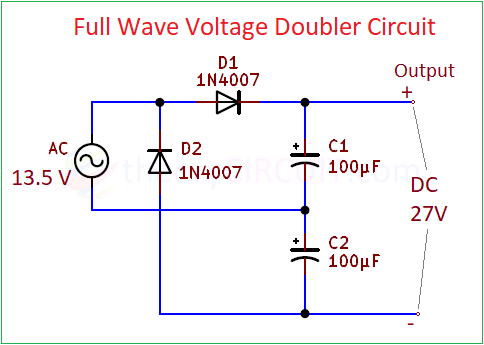
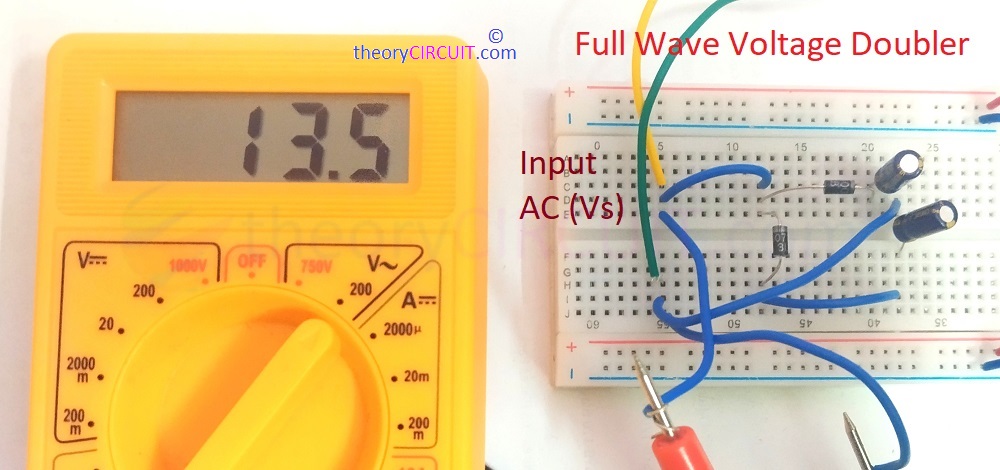
- AC Voltage Source., (we have taken 0-12Vac Step down Transformer – But received 13Vac)
- Diode 1N4007 = 2
- Electrolytic Capacitor 100μF/25V = 2
- Breadboard
- Connecting Wires
Half Wave Voltage Doubler
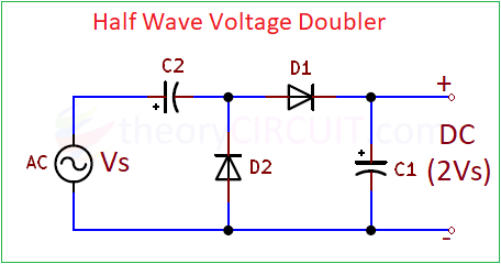
Construction & Working
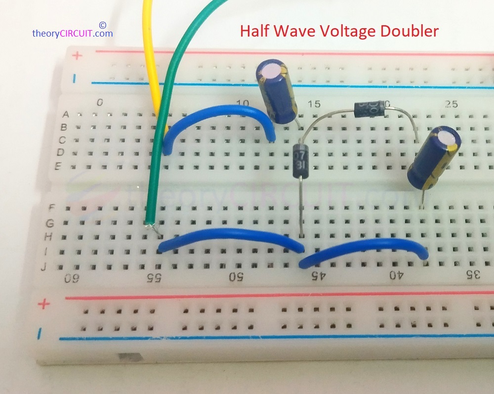
To Construct Halfwave Voltage doubler you need pair of PN Diode and Pair of Electrolytic capacitor, always choose electrolytic capacitor with voltage rating that meets the output dc voltage from the doubler circuit. Connect AC source with components as mentioned in the circuit, use multimeter to check the input AC supply and output DC supply.
After wiring done, lets turn on the circuit and analyse how it doubles the voltage, During the Negative cycle of Input AC signal (VS) the diode D2 starts to conduct after 0.7V in forward bias and charges the C2 capacitor. During Negative cycle D1 stays in Reverse bias so there will be no conduction in D1 and C1 don’t get charged. There is no discharge path to C2 so the Charge up to Vs stays in C2.
When the positive cycle arrives suddenly, The diode D2 goes to Reverse bias and D1 gets forward bias after 0.7V and the C2 capcitor Charge Vs also finds discharging path through D1 and the C1 Capacitor now receives 2Vs charge, so the output will be 2*Vs in DC.
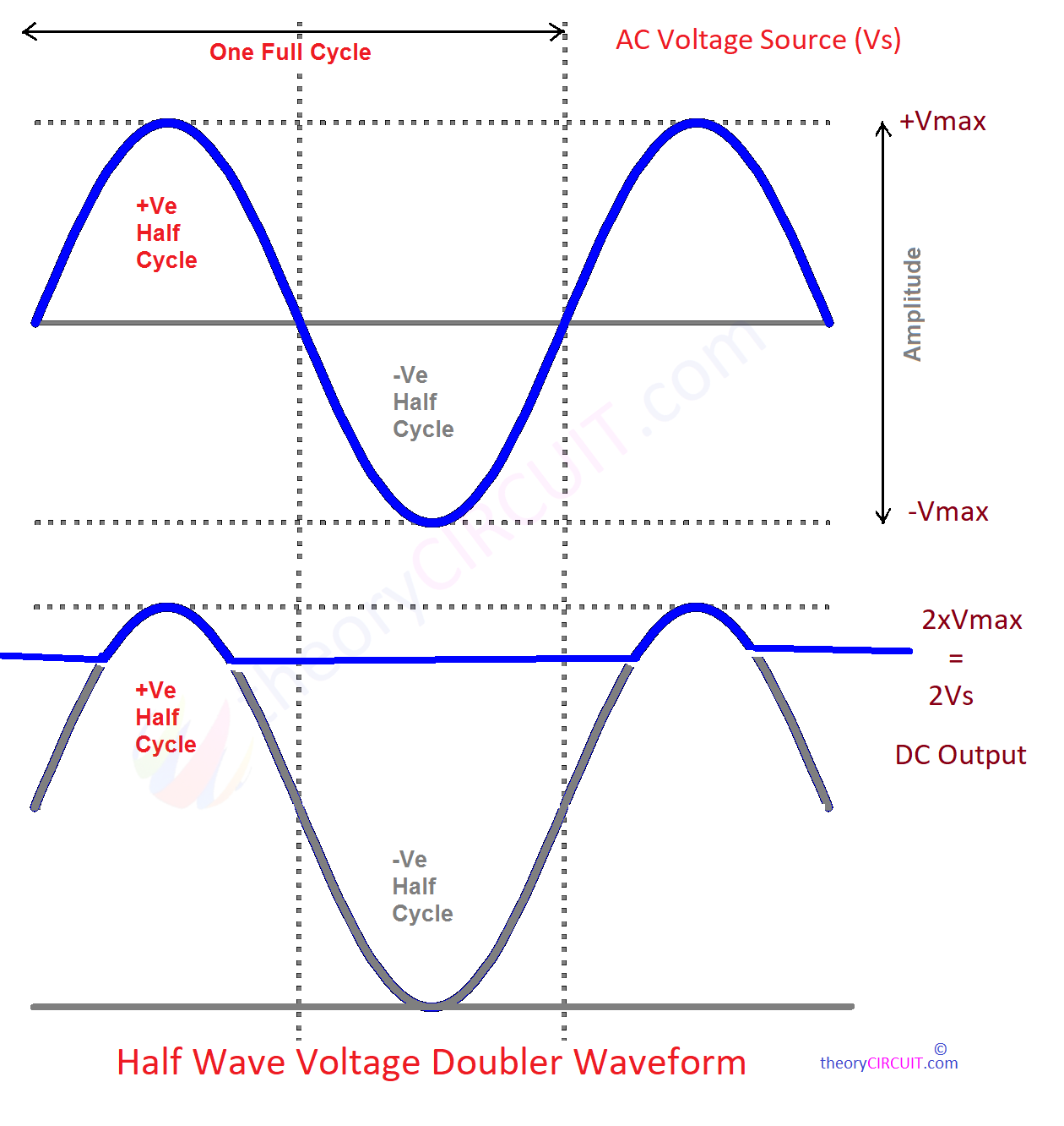
Half Wave Voltage Doubler Waveform
Testing Result
Full Wave Voltage Doubler
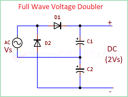
Construction & Working
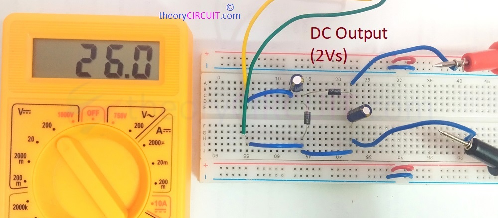
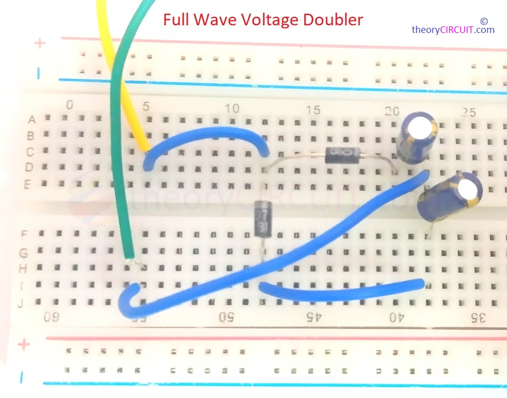
Here also you need pair of PN diode and pair of Electrolytic Capcitor for Full Wave voltage doubler, Output is taken from the end terminals of two serially connected capacitors. After making connection lets turn on and analyse the operation.
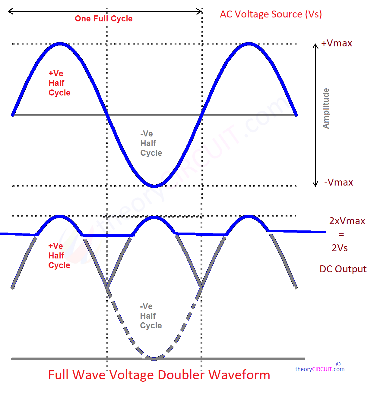
During the Positive half cycle from AC voltage source (Vs), the Diode D1 starts conducting after 0.7V in forward condition, and charges Capacitor C1 up to Vs level. During this time D2 stays in reverse bias. So the C2 capacitor don’t get charged.
During the Negative half cycle from AC Voltage Source (Vs), the diode D2 starts conducting in forward bias and charges Capacitor C2 up to Vs level. During this time D1 stays in Reverse bias. Now both Capacitor C1 and C2 charged up to Vs + Vs levels, here these two capacitors in series connection so the output will be 2*Vs DC appears.
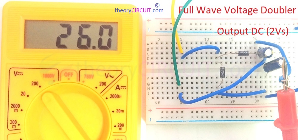
For both half and full wave voltage doublers output will be 2*Vs during the no load condition, when we connect load output will be slightly decreased from its maximum level and the full wave type gives maximum efficiency.
Full Wave Voltage Doubler Waveform
Testing Result
Hi.
Half Wave Voltage Doubler
– will this circuit work with a water meter?
The pulses at the meter output are 5.4V, 10mA, frequency 70-90Hz.
Thanks.