
Last Updated on March 29, 2024
As we know Operational Amplifiers, Sensors and some Signal Conditioning circuits requires Negative Voltage as bias and reference voltage. Adding hardware for to get negative voltage will increase the size of circuit and cost. Here is the simple and easy method to get it through Negative Voltage Generator Circuit using IC 555.
When you need constant negative voltage as bias, you can use negative rectification and negative linear voltage regulators or dual rail power supply circuit. In some cases we need changeable negative voltage as reference for microcontrollers, Sensor or signal conditioning circuit. In that situation you can use this type of Negative voltage generator and you can vary the output voltage as you want, by changing the timer IC 555 output frequency.
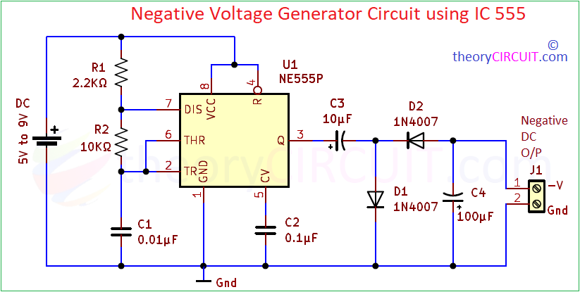
Circuit Diagram
Components List
- Timer IC 555
- Resistor 2.2KΩ, 10KΩ each one
- Capacitor 0.01μF, 0.1μF each one
- Electrolytic Capacitor 10μF, 100μF each one with 16 Volt rating
- Diode 1N4007 = 2
- DC supply
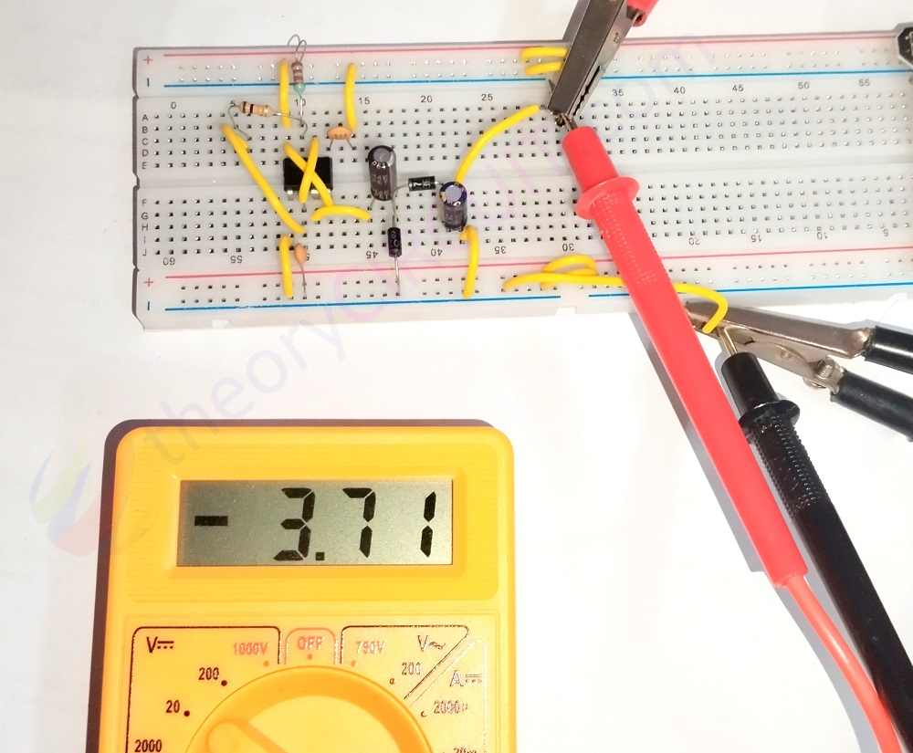
Prototype
Negative Voltage Generator Circuit using IC 555 prototype
This circuit generates negative voltage rail and makes dual rail from single rail supply.
Construction & Working
Operation of this circuit occurs in two parts one is oscillator another one is charging and discharging through Capacitor. Here diode D1, D2 (1N4007) helps to allow and block flow of changing potential from capacitors.
As you found this circuit uses timer IC 555 in Astable Multivibrator mode and generates square pulse output depends on the timing Resistor (R1, R2) and timing capacitor C1 values.
f = 1.44 / (R1+2R2)*C1
In the above circuit output pulse frequency f is,
f =1.44/(2200+210000)0.00000001
f =1.44/0.000222
f =6486.48 Hz
f =6.4 KHz
Astable Multivibrator Circuit Calculator.
Here we picked components to produce -3.7V (negative) output. Change the Value of R1, R2 and C1 to get different range of output, remember output voltage is limited to maximum Vcc applied to timer IC 555.
lets continue to the working details, In the square pulse output there will be positive pulse duration and ‘0’ or Ground pulse duration.
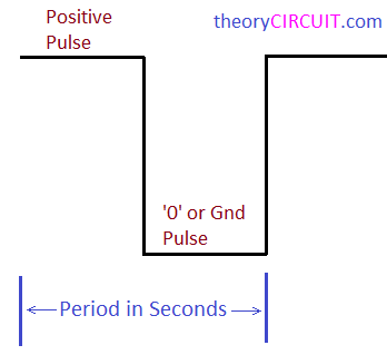
When the positive pulse duration appears on pin 3 (Output of timer IC 555) the voltage steps up from 0 to half Vcc, during this time period capacitor C3 Positive plate gets charge, due to capacitive coupling negative plate also get charged, when the negative plate of C3 reaches 0.7V then the diode D1 starts conducting in forward bias. So the positive plate of C3 stays in half of Vcc and negative plate stays at 0.7V because of diode D1.
When the ‘0’ or Ground pulse appears, Capacitor C3 positive plate suddenly drops from half of Vcc to ‘0’ so there will be half Vcc potential difference maintained due to capacitive coupling of two plates. Then the Negative plate drops to -Ve Half Vcc and it cannot be conducted by diode D1 due to reverse bias, but D2 starts conducting due to forward bias and C4 gets Negative Potential charge and it smoothens output voltage (Negative), this cycle repeats and we get constant negative voltage output.