Last Updated on August 27, 2025
Equalizer circuit in a Audio System helps us to filter & adjust Bass, Mid, Treble frequencies. Sometimes while listening to Audio, you may felt the low bass or too sharp treble like noise. Then we adjust some knobs (Audio Equalizer) to get proper sound. Here the Audio Equalizer circuit makes filtering in the Audio source signal before it reaches Audio Amplifier so that we get expected output through loud speaker.
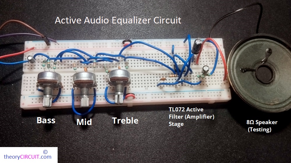
Let’s design simple and useful 3 band Active Audio Equalizer circuit using IC TL072. This circuit allows for independent control of bass, mid range and treble frequencies, making it ideal for preamplifier and DIY Hi-Fi upgrade to simple audio amplifiers. Unlike passive circuit, this Active Equalizer circuit provides gain to filtered frequencies and attenuate others. Either you can build this circuit on Veroboard or use the PCB Gerber file.
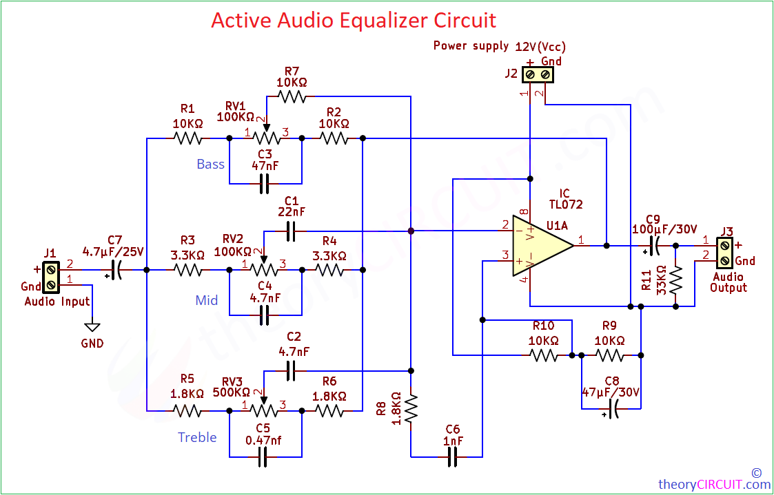
Circuit Diagram
Components Required
| 1 | C2, C4 | 4.7nF | C_Disc_D3.8mm_W2.6mm_P2.50mm | 2 | ||
| 2 | C1 | 22nF | C_Disc_D3.8mm_W2.6mm_P2.50mm | 1 | ||
| 3 | C3 | 47nF | C_Disc_D3.8mm_W2.6mm_P2.50mm | 1 | ||
| 4 | C5 | 0.47nf | C_Disc_D3.8mm_W2.6mm_P2.50mm | 1 | ||
| 5 | C6 | 1nF | C_Disc_D3.8mm_W2.6mm_P2.50mm | 1 | ||
| 6 | C7 | 4.7μF/25V | CP_Radial_D4.0mm_P2.00mm | 1 | ||
| 7 | C8 | 47μF/30V | CP_Radial_D4.0mm_P2.00mm | 1 | ||
| 8 | C9 | 100μF/30V | CP_Radial_D4.0mm_P2.00mm | 1 | ||
| 9 | R1, R2, R7, R9, R10 | 10KΩ | R_Axial_DIN0207_L6.3mm_D2.5mm_P10.16mm_Horizontal | 5 | ||
| 10 | R5, R6, R8 | 1.8KΩ | R_Axial_DIN0207_L6.3mm_D2.5mm_P10.16mm_Horizontal | 3 | ||
| 11 | R3, R4 | 3.3KΩ | R_Axial_DIN0207_L6.3mm_D2.5mm_P10.16mm_Horizontal | 2 | ||
| 12 | R11 | 33KΩ | R_Axial_DIN0207_L6.3mm_D2.5mm_P10.16mm_Horizontal | 1 | ||
| 13 | U1 | TL072 | DIP-8_W7.62mm_LongPads | 1 | ||
| 14 | RV1, RV2 | 100KΩ | Potentiometer_Alps_RK163_Single_Horizontal | 2 | ||
| 15 | RV3 | 500KΩ | Potentiometer_Alps_RK163_Single_Horizontal | 1 | ||
| 16 | J1 | Audio Input | TerminalBlock_Altech_AK300-2_P5.00mm | 1 | ||
| 17 | J2 | 12V | TerminalBlock_Altech_AK300-2_P5.00mm | 1 | ||
| 18 | J3 | Audio | TerminalBlock_Altech_AK300-2_P5.00mm | 1 |
Working Video
Circuit Construction
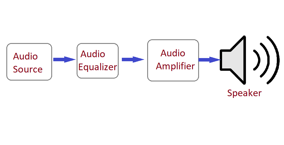
Audio Equalizer circuit is positioned between Audio Source and Audio Amplifier, It allows desired frequency signal to get different acoustic effect from speaker and cuts other frequency signal from input source.
This circuit uses IC TL072 (Dual op-amp) as a main Active Element to provide filtering gain to Audio Signal.
TL072 Pinout
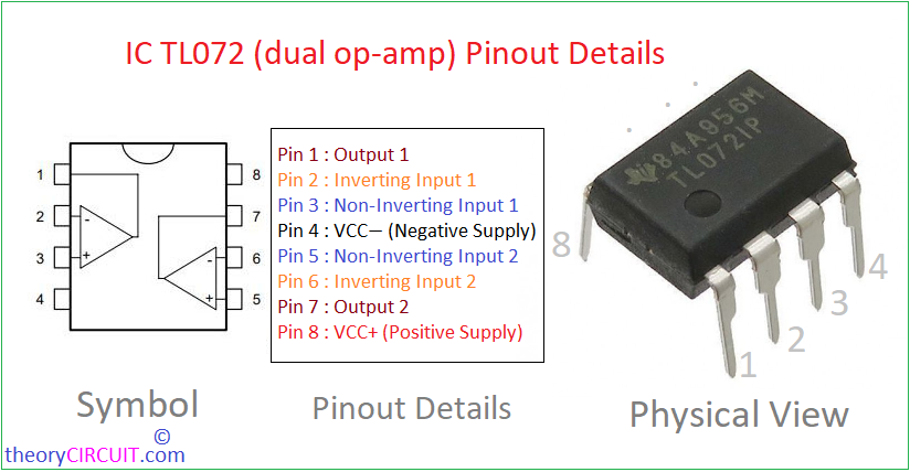
Single op-amp (U1A) from TL072 is being used in this circuit. If you need to buffer audio signal, you can use another op-amp (U1B) from TL072.
U1A op-amp in an inverting configuration with frequency selective feedback networks performs active equalizing in Audio signal. Here the input signal enters through DC blocking coupling capacitor C7, gets filtered through parallel RC Networks controlled by potentiometers for each band and flows to inverting input of U1A operational amplifier then exits via another coupling capacitor C9 to the speaker (It should go to amplifier – here we directly connected to 8Ω speaker for testing).
This circuit inspired from the Baxandall (Base and all 😉 ) tone control topology but extended it to three band by adding mid range peak filter. Here the op-amp provides unity gain when the pots are centered, with up to +/- 15dB boost or cut depending on pot values.
This circuit is designed with the following terms in mind.
Bands : Bass (Low pass shelf), Mid (Band pass peak/dip), Treble (High pass shelf).
Power Supply : Single rail 12V with mid rail biasing for Audio signal handling by op-amp.
Controls : Three linear potentiometers (Pots) for Boost and Cut.
This circuit uses single Op-Amp and few external components to keeping it compact and low cost to build.,
Circuit Operation
Here this circuit operates on the principle of frequency dependent negative feedback in an inverting op-amp configuration. Input Stage starts with C7 (4.7μF) capacitor which blocks DC and allows Audio Signal to RC Networks. Here the cut off frequency of RC Network can be calculated as,
fc = 1/(2πRC)
For Bass RC Network fc will be calculated as,
fcbass = 1/(2π*(R2+RV1+R7)*C3
For Mid RC Network fc will be calculated as,
fcmid = 1/(2π*(R4+RV2)*C1)
For Treble RC Network fc will be calculated as,
fcmid = 1/(2π*(R6+RV3)*C2)
Inverting Amplifier with EQ Feedback
Audio Input reaches the inverting input pin 2 through variable pins of potentiometers followed by R7, C1, C2. Then the feedback from output pin 1 to pin 2 is split into three parallel paths,
- Bass feedback path : R2 -> RV1 (with parallel C3) -> R7.
- Mid feedback path : R4 -> RV2 (with parallel C4) -> C1.
- Treble feedback path : R6 -> RV3 (with parallel C5) -> C2.
When the pots are at center (50 % Resistance) then the circuit approximates unity gain then turning clockwise Increase Resistance in the path hence Increasing feedback (cut), counter clockwise decreasing it (Boost).
Biasing to this circuit is single rail 12V supply, that is (12V, GND) in order to handle negative peak in audio signal we introduce offset to op-amp non inverting pin through R9 – R10 Voltage divider. Hence the Vcc/2 ~ 6V is applied to non inverting pin 3 of U1A. This will allow op-amp to handle bipolar Audio signals around this virtual ground. Here C8 decouples the power noise.
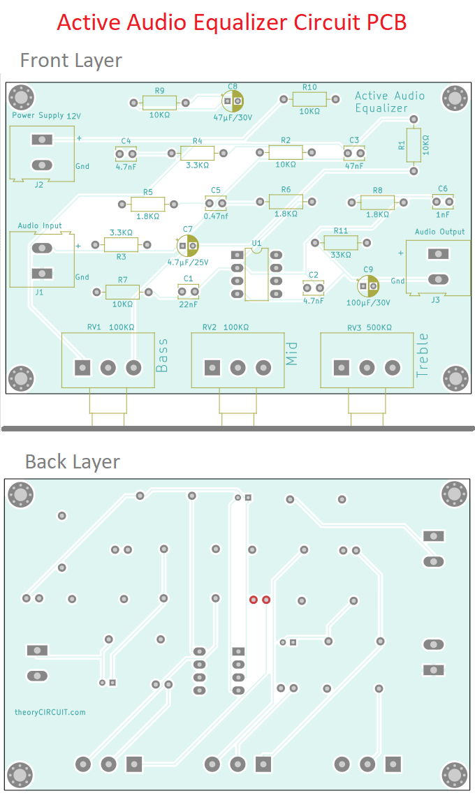
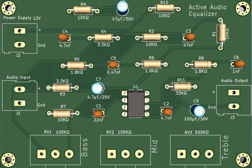
Printed Circuit Board
Active Audio Equalizer Circuit PCB Gerber Files.
Interactive Board Viewer


PCB 3D View
Audio Equalizer circuit on Breadboard