Last Updated on March 16, 2024
If we need High voltage from low voltage power source then we use traditional DC-DC boost converter circuit, but the problem is those circuits are bulky and makes the circuit design more complex. In this prototype design we use compact and powerful boost converter from Analog Devices IC LT8330. This boost converter takes low input power source and gives High voltage output with minimum external components.
IC LT8330 is current mode DC/DC boost converter capable of generating either positive or negative output voltages using a single feedback pin. It consumes 6μA quiescent current only. Positive or Negative output can be programmed by the single feedback pin. This IC has fixed 2MHz switching frequency.
Circuit Diagram
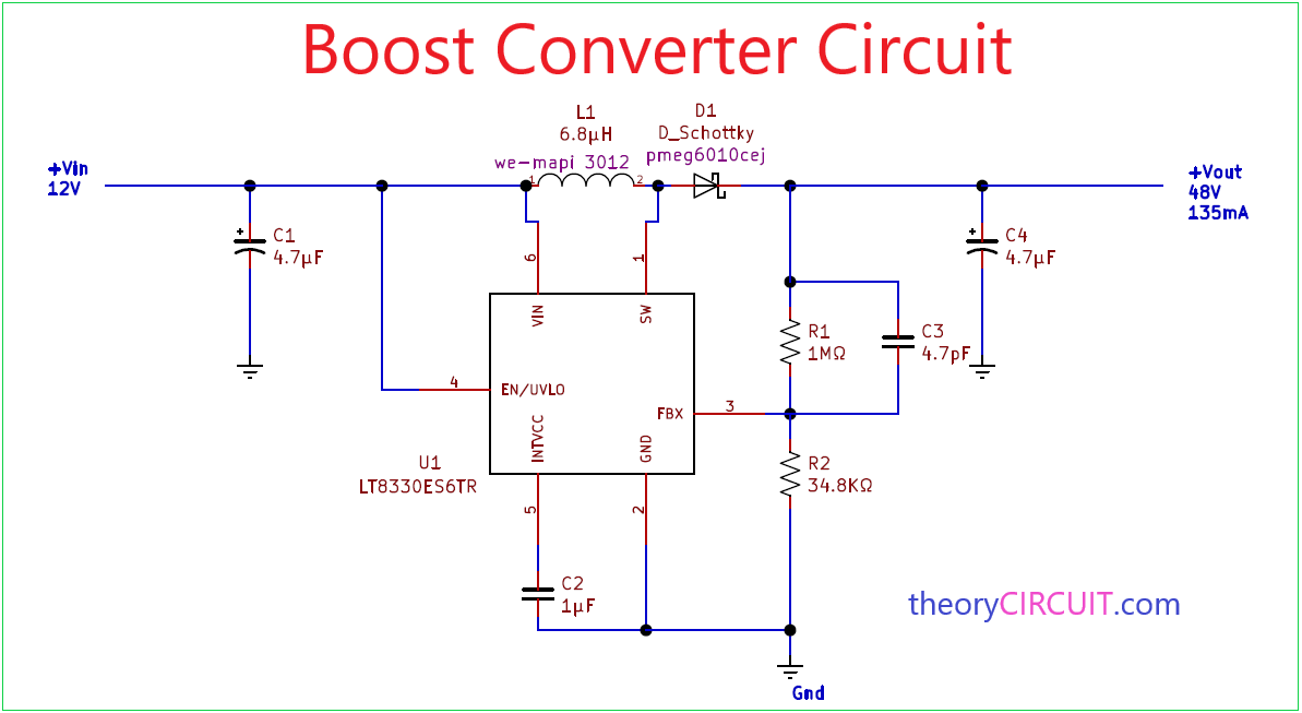
Components Required
- IC LT8330ES6TR
- Capacitor 4.7μF = 2
- Capacitor 1μF, 4.7pF each one
- Resistor 1MΩ, 34.8KΩ each one
- Inductor 6.8μH
- Schottky diode (pmeg6010cej)
Circuit Assembly & Operation
All components represented in circuit diagram are SMD components and its better to assemble in printed circuit board.
IC LT8330 can take 3V to 40V input as input voltage range, This IC can be configured as Boost, SEPIC or inverting converter with very low quiescent current. With the help of internal compensated current mode architecture this IC gives stable operation over wide range of input and output voltages.
IC LT8330 Pin Configuration
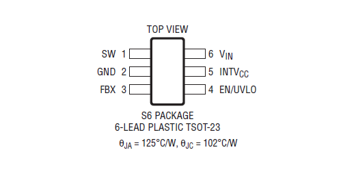
SW: The Output of Internal Power Switch Pin. GND: Ground Connection Pin.
FBX: Voltage Regulation Feedback Pin for Positive or
Negative Outputs. EN/UVLO: Shutdown and Undervoltage Detect Pin. INTVCC: Regulated 3V Supply for Internal Loads Pin. VIN: Input Supply Pin.