Last Updated on April 16, 2024
The full adder circuit diagram add three binary bits and gives result as Sum, Carry out. It can be used in many applications like, Encoder, Decoder, BCD system, Binary calculation, address coder etc.., the basic binary adder circuit classified into two categories they are
- Half Adder
- Full Adder
Here three input and two output Full adder circuit diagram explained with logic gates circuit and also logic IC Circuits.
Full Adder
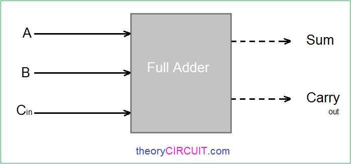
The full adder will take three inputs named as A, B, Cin then it will give two outputs named as Sum, Carry out.
- Sum = A⊕B⊕Cin
- Carry out = A.B + (A⊕B).Cin
The result sum is exclusively addition between A,B,Cin then result carry is OR logic operation between A.B then A⊕B and Cin.

Full Adder Logic Gate Diagram
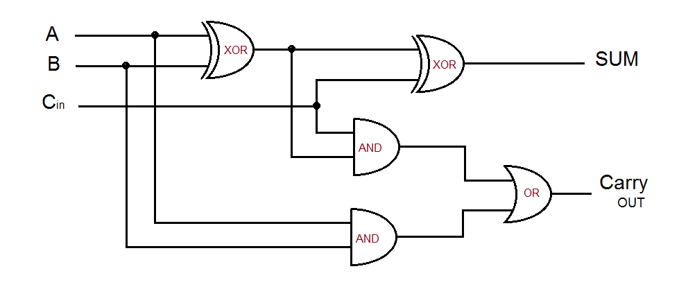
Two input XOR gate, two input AND gate, two input OR gate forms the full adder logic circuit, Input & Output of this logic diagram can be derived by the following truth table.
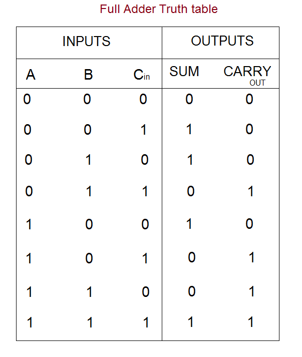
When both inputs are low then sum and carry out will be logic low (0), if any one input is high then sum will be logic high (1) and carry out will be logic low (0), when two inputs are high then sum becomes logic low (0) and carry out becomes logic high (1) when all inputs are high (1) the output sum and carry out will be logic high (1).
Full Adder Circuit Diagram

Full Adder Working Video
Components List
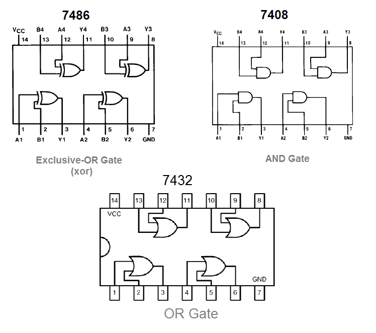
- EXOR Gate IC 7486
- AND Gate IC 7408
- OR Gate IC 7432
- Green LED (for Sum Result)
- Red LED (for Carry Result)
- Resistor 330Ω = 2
- Breadboard
- Jumper Wires
- 5V DC Power supply
Construction & Working
Here XOR gate IC 7486 and Logic AND gate IC 7408 and OR gate IC 7432 are used to construct the full adder circuit, both are quad 2 input logic gate IC. First connect Vcc +5V and GND supply to logic IC, Input A, B is connected to the XOR gate input then AND gate input, output of first XOR gate (Pin 3) is connected to the next XOR gate input pin 4 and Cin connected to XOR gate input pin 5. Second AND gate takes A⊕B, Cin as inputs. XOR gate pin 6 taken as Sum Result and connected to LED1 through R1. Two AND gate outputs are added by OR gate then OR gate pin 3 taken as Carry out output and connected to LED2 through R2 resistor. After making the connection verify the full adder truth table. When LED glows it represents logic High (1), during OFF condition LED represents logic Low (0).
IC 7486 – IC 7408 – IC 7432 pinout
Note:-
* Connect Input A, B, Cin to +Vcc for logic High (1) input.
* Connect Input A, B, Cin to GND for logic Low (0) input.
* Some times open A, B, Cin terminal represents logic High.
* Use different Color LEDs to represent Sum and Carry.
* If you are building this full adder circuit in breadboard then check each contact terminals before verifying truth table.
What software/ online tool has been used to design the above pin diagram?