Last Updated on November 20, 2024
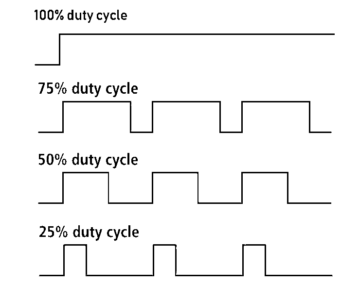
By using Timer IC 555 we are going to design Adjustable Duty Cycle PWM Generator Circuit. Before that, What is Duty Cycle and PWM? Here is the answer in simple words. In a pulse, Percentage of ON (HIGH) time (period) is called as Duty Cycle. In a pulse, Width of pulse is (either ON or OFF time) Varies depends on the Input signal means that is called as Pulse Width Modulation (PWM) signal. PWM signal is classified into two categories based on their application.
- PWM in Communication technique, uses Carrier and Message.
- PWM as Control Signal, uses Pulse Oscillation and Input.
Different Duty Cycle range in a Pulse, shows the ON (HIGH) time duration changes.
Here our aim is to build Adjustable Duty Cycle PWM signal for the purpose of controlling speed of motor, Brightness of LED, Servo Motor control or Power Electronics utilization. So we use PWM as Control Signal. In a pulse oscillator an variable resistor (potentiometer) can be used to adjust the Duty Cycle/PWM. Well familiar 555 Astable Multivibrator circuit also uses timing element as Resistor and Capacitor, by replacing a Resistor into Variable Resistor gives control to change the pulse duration.
Adjustable Frequency / Duty Cycle PWM Generator Circuit
Components Required
- Timer IC: NE555P
- Diodes: 1N4007 (2 pieces)
- Resistors: 1 KΩ (2 pieces)
- Variable Resistor: RV1: 10 KΩ
- Capacitors: 0.1 µF (2 pieces)
- LED: General-purpose LED (1 piece)
- Power Supply: +5V to +9V
Working Video
Construction & Working
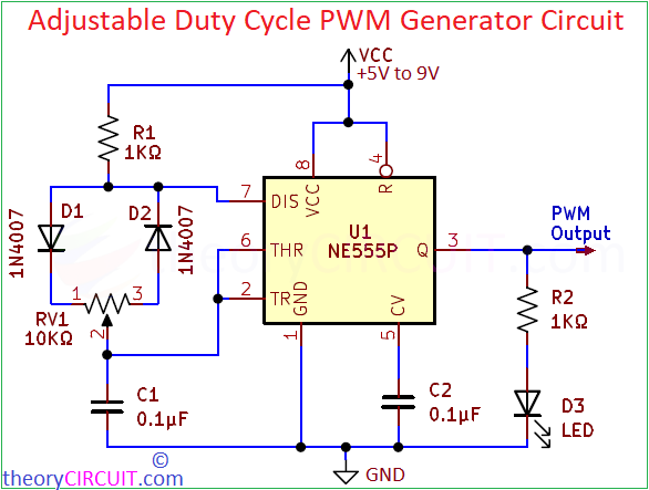
Here this circuit configured in Astable Multivibrator mode, to generate square pulse but the discharge path to the timing Capacitor have variable Resistor RV1. So the pulse duration is decided by the value of timing Capacitor C1 and RV1. When its power on, Capacitor C1 gets charge through Resistor R1, Diode D1 and lower part (RV1L) of Variable Resistor RV1 (Resistance between 1 and 2 pin). During the charging time and upto 1/3 Vcc, the internal lower comparator sets the Flip Flop output “HIGH”, when the capacitor reaches 2/3 Vcc then the internal upper comparator resets the Flip Flop and resets output “LOW”. It leads to discharging the capacitor and makes time duration of LOW pulse.
C1 Capacitor discharge through Upper part (RV1U) of RV1 ( Resistance between 2 and 3 pin), Diode D2. By changing this variable Resistor value we can control the Charging & Discharging time of C1. It can be written as,
TON = 0.693*(R1+RV1L)*C1
TOFF = 0.693*(RV1U)*C1
T = TON+TOFF
Duty Cycle can be written as,
D = (TON / T ) * 100
By varying RV1, Charging time (TON) and discharging time (TOFF) can be changed, it gives control over the duty cycle.
Here the output frequency also slightly change due to the RV1, if you want to have fixed frequency with Adjustable Duty Cycle PWM then use the following circuit.
Components Required
- Timer IC: NE555P
- Diode: 1N4007 (2 pieces)
- Resistor: 10 KΩ (2 pieces), 1 KΩ (1 piece)
- Variable Resistor: 100 KΩ (1 piece)
- Capacitor: 0.1 µF (2 pieces)
- LED: General-purpose LED (1 piece)
- Power Supply: +5V to +12V
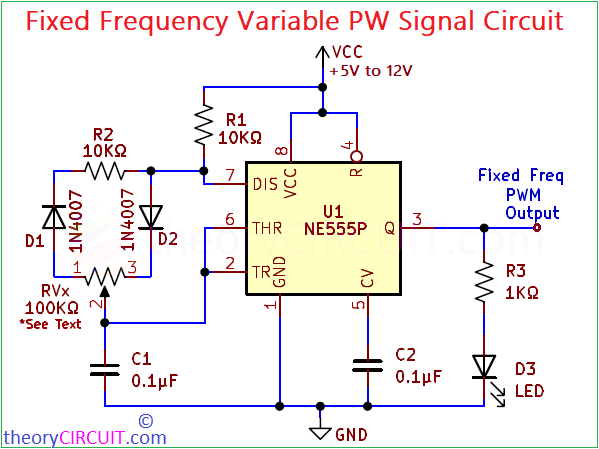
This circuit generates PWM signal with fixed frequency and adjustable duty cycle using the timer IC NE555P. It is configured in Astable Multivibrator mode. Here RVX Variable Resistor works as Lower part RVL (Resistance between pin 1 and wiper pin 2) and Upper part RVU (Resistance between wiper pin 2 and pin 3). This circuit also works in the same way as previously said. But the Charging and Discharging path of C1 becomes,
C1 Charging = Vcc -> R1 -> D2 -> RVU (pin 3 to pin 2)
C1 Discharging = RVL (pin 2 to pin 1) -> D1 -> R2 -> 555 DIS pin 7
TON = 0.693*(R1+RVU)*C1
TOFF = 0.693*(RVL+R2)*C1
T = TON+TOFF
F = 1/T
Duty Cycle can be written as,
D = (TON / T ) * 100
You can change the RVU and RVL pins of variable resistor.
Due to fixed On time Ton and Off time Toff, we can get fixed frequency output and the RVx controls the pulse width (duty cycle).
Note: Calculate the total value of RVx = RVL + RVU, for an example if you have 100 KΩ RVx then total value of RVL + RVU should be 100 KΩ.


