Last Updated on December 17, 2024
When Someone ask what are Universal logic Gates? We immediately say NAND & NOR. This because we can construct any logic gate and Boolean function without need for any other logic gates using NOR & NAND. We know that logic gate are the building blocks of digital electronics. So by designing logic gates using transistor we can easily understand the logic operations of Logic Gate with truth table and we can customize logic design using Transistor (BJT – Bipolar Junction Transistor) and understand how logic IC functions inside.
NOR Gate with Truth Table
NOR Gate gives HIGH (1) output only when both inputs are LOW (0). It makes operation of OR gate followed by a NOT gate. Boolean expression for NOR logic gate is
So it makes Addition between A, B inputs then makes complement.
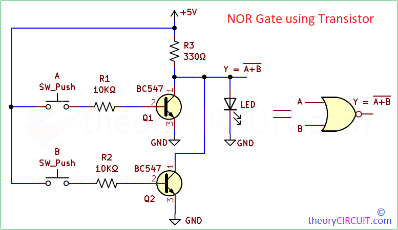
NOR Gate using Transistor
To make NOR Gate you can use any NPN Switching Transistor like (BJT – BC547, 2N2222 and MOSFET) here we used most commonly available BC547 Transistor.
Required Components
| S.No | Component | Value / Specification | Quantity | Description |
|---|---|---|---|---|
| 1 | Transistor (Q1, Q2) | BC547 (NPN) | 2 | General-purpose NPN transistors |
| 2 | Resistor (R1, R2) | 10 KΩ | 2 | Base current limiting resistors |
| 3 | Resistor (R3) | 330 Ω | 1 | Pull-up resistor for output |
| 4 | Push-Button Switch | Normally Open (NO) | 2 | Input switches (A & B) |
| 5 | LED | Standard Red LED | 1 | Output indicator |
| 6 | Power Supply | +5V DC | 1 | Power source |
| 7 | Connecting Wires | – | As required | For circuit connections |
| 8 | PCB/ Breadboard | – | 1 | For mounting the components |
Working Video
Circuit Operation
A NOR Gate with two inputs can be build using two NPN transistor connected in parallel. Both transistor Q1, Q2 Base terminal will act as Inputs (A, B). Both Transistor collector terminal is connected to a pull-up Resistor (R3) and then to positive supply (Vcc). This VCC level decides HIGH (1) so make it up to 5V. If you need, you can make it 3.3V logic also. Both transistor emitter terminals are connected to Ground (GND). Output Y is taken from the junction of the collectors and the pull-up Resistor (R3). To show the output we used an LED. When both inputs (A, B) are LOW (0) Q1, Q2 stays in OFF condition so there is no conduction to Ground. So the pull up resistor R3 pulls the output HIGH (1). Any one or both inputs (A,B) are HIGH (1) then the Q1, Q2 or any one transistor gets enough base supply and starts to conduct positive to ground. So there is no bias at the output and output Y becomes LOW (0).
NAND Gate with Truth Table
NAND Gate gives LOW (0) output only when both inputs are HIGH (1). It makes operation of AND gate followed by a NOT gate. Boolean expression for NAND logic gate is
So it makes logic multiplication between A, B inputs then makes complement.
NAND Gate using Transistor
To make NAND Gate you can use any NPN Switching Transistor like (BJT – BC547, 2N2222 and MOSFET) here we used most commonly available BC547 Transistor.
Circuit Operation
A NAND Gate with two inputs can be build using two NPN transistor connected in series. Both transistor Q1, Q2 Base terminal will act as Inputs (A, B). Q1 Transistor collector terminal is connected to a pull-up Resistor (R3) and then to positive supply (Vcc). This VCC level decides HIGH (1) so make it up to 5V. If you need, you can make it 3.3V logic also. Q1 transistor emitter terminals is connected to Q2 Transistor Collector terminal making to series and then Q2 transistor emitter terminal to Ground (GND). Output Y is taken from the junction of the Q1 collector and the pull-up Resistor (R3). To show the output we used an LED. When both inputs (A, B) are HIGH (1) Q1, Q2 gets enough base bias and starts to conduct supply between collector to emitter that is ON condition, so the Vcc gets to Ground. So there is no bias at the output and output Y becomes LOW (0). Any one or both inputs (A, B) are LOW (0) then Q1, Q2 or any one transistor stays in OFF condition. So there is no conduction of Vcc to Ground. Then the pull up resistor R3 pulls the output HIGH (1).


