
Last Updated on March 16, 2024
The 433MHz RF Tx Rx module (Transmitter and Receiver modules) possesses the capability to transmit data sequences without wires within a range of 100 meters. Crafting a straightforward wireless switch involves a single push button input. If you’re pondering how to integrate a 433MHz RF Transmitter and Receiver into a circuit with numerous switch inputs and outputs, the solution lies in employing IC HT12E (Encoder) and IC HT12D (Decoder). This combination allows the realization of multiple inputs and outputs within the 433MHz RF Transmitter and Receiver circuit. This module use Amplitude Shift Keying method to convert input data signal into RF that is why this is called as ASK RF Module circuit diagram.
433MHz Transmitter module some times termed as FS1000A Module and it takes sequence binary input (Logic HIGH and LOW) and modulates it in Amplitude Shift Keying and propagates as RF signal (Radio Frequency). The reverse operation happens in 433MHz Receiver module and gives sequence binary output. When we introduce Encoder and Decoder we can increase the ability of these module and get multiple input and output at the same time.
433MHz ASK RF Module Pinout
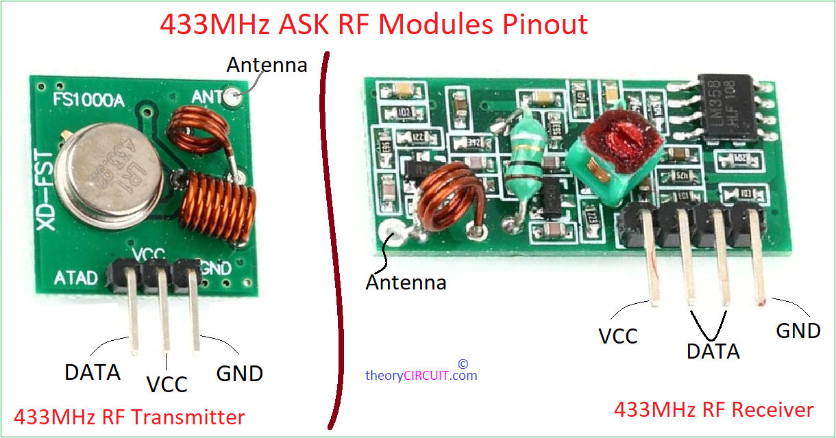
Refer FS1000A 433MHz RF transmitter and receiver Brief Note for full details. Lets Jump into the Circuits.
ASK RF Module Transmitter Circuit
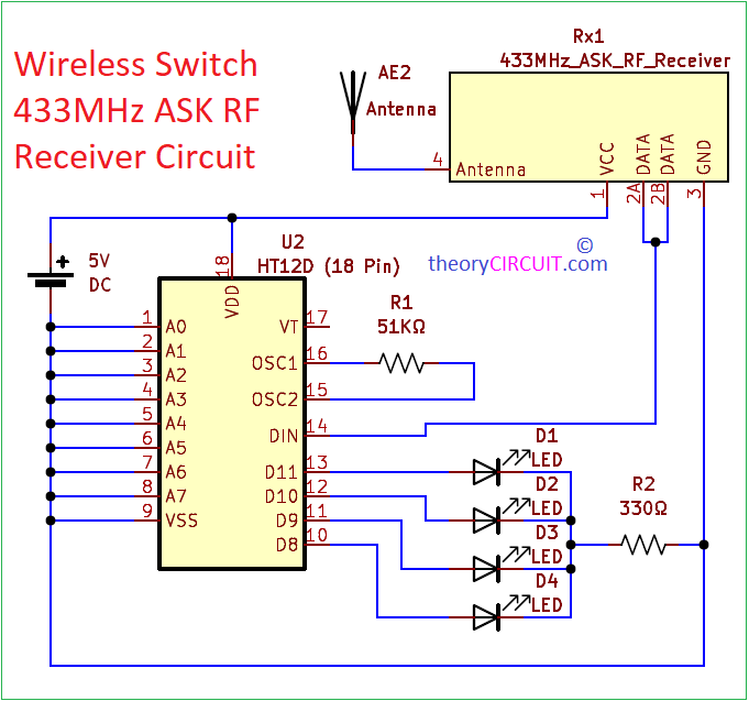
ASK RF Module Receiver Circuit
Components List
- FS1000A 433MHz ASK RF Transmitter and 433MHz Receiver Module.
- IC HT12E (18 Pin Dip)
- IC HT12D (18 Pin Dip)
- Four Pushbutton Switch
- Four LED (any color)
- Resistor 1MΩ, 51KΩ, 330Ω
- Power supply
Construction & Working
The Transmitter and Receiver circuits are built independently. In both the Encoder and Decoder ICs, the Address lines are grounded and set to 00000000. In the Encoder IC HT12E, the Transmission Enable (TE’) is connected to Ground, maintaining it in a LOW state as it is an active low pin. To generate a 3KHz pulse signal in the internal oscillator, a 1.1MΩ external resistor is required. In our setup, a 1MΩ external resistor is utilized, and it functions well. Meanwhile, for the Decoder IC HT12D, the external resistor for the oscillator is 51KΩ.
AD8 to AD11, four pins in the Encoder IC connected with input push button switch, when the Switch is open it is considered as HIGH input and when the switch is pressed then it is considered as LOW input because the other end of switch is connected with Ground supply. you can Invert this by connecting diode in reverse then pushbutton switch to these Data input pin.
In the Receiver circuit, following ASK demodulation, the Decoder IC receives a sequence of data through the DIN pin. Once the HT12D Decoder IC captures the data sequence, its internal circuit processes the signal, distinguishing between address bits and data bits. Subsequently, it conducts a comparison between the received address bits and its pre-set address to ascertain if the data is meant for it. If there’s a match in addresses, the data is directed to the output pins, leading to the illumination or turning off of the LED based on the wirelessly transmitted data.