
Last Updated on March 16, 2024
Simple Wireless LED Circuit build by using Timer IC 555 and buck/boost regulator IC MC34063, it can be used as general purpose power transmitter and receiver, In this circuit small value of power is transferred from transmitter to receiver coil using inductive coupling method. This kind of wireless power transfer works efficiently only in the transmitter and receiver coil aligned properly in terms of distance and frequency.
Nowadays Wireless power transfer needs are increasing rapidly, Let us look into some of diverse applications across various industries. In consumer electronics, it enhances user convenience by enabling wireless charging for smartphones and wearables. The medical field benefits from wireless power in implantable devices, reducing the need for frequent surgeries. The automotive industry embraces this technology for electric vehicles and buses, simplifying the charging process. In the IoT, sensors in remote locations and smart homes leverage wireless power for seamless operation. Industrial automation and robotics witness increased efficiency through wirelessly powered sensors and actuators. So it is beneficial to experiment wireless power transfer techniques.
Circuit Diagram
Construction & Working
Wireless Power Transmitter
Wireless power Transmitter circuit is Constructed by using Timer IC 555 in Astable Multivibrator Configuration to Produce 20KHz Square pulse. Here the timing components (Resistors) R1, R2 and (Capacitor) C1, gets charging and discharging continuously and creates continuous cycle of oscillation. Here VCC pin and Reset pin connected with positive supply, R1 resistor is connect between Discharge pin and positive supply, R2 resistor is connected between discharge pin and Shorted Threshold, Trigger pin. C Capacitor is connected between (THR, TR) pin and GND.
The capacitor C1 begins to charge through Resistor R1 then Discharge pin 7 and R2, as the voltage across the capacitor reaches 2/3 of the Power supply (VCC) then the internal flip flop of the 555 timer changes its state, this causes the discharge pin 7 to go LOW and then the Capacitor C starts to discharge through Resistor R2 and the discharge pin 7. When the voltage across the capacitor decreases to 1/3 of power supply (VCC) then the internal flip flop changes its state again and the Discharge pin 7 goes HIGH, this cycle of charging and discharging repeats and generates Continuous Square pulse at output pin.IRF540 N-Channel MOSFET receives square pulse in Gate terminal and acts as Switch, that is it turn ON during positive pulse and turn OFF during negative pulse. Hence Coil L1 Connected with Drain terminal gets discrete (ON and OFF) supply, and produce strong fluctuating electromagnetic field.
Copper Coil Setup
Insulated copper wire with 18 SWG winded 25 turns and used as Power Transmitter coil, this coil will make strong electromagnetic flux by using high frequency square pulse from timer IC 555. Receiver Coil made with 22 SWG insulated copper wire and winded 100 turns, this coil will make current flow and potential difference depends on the received electromagnetic fields.
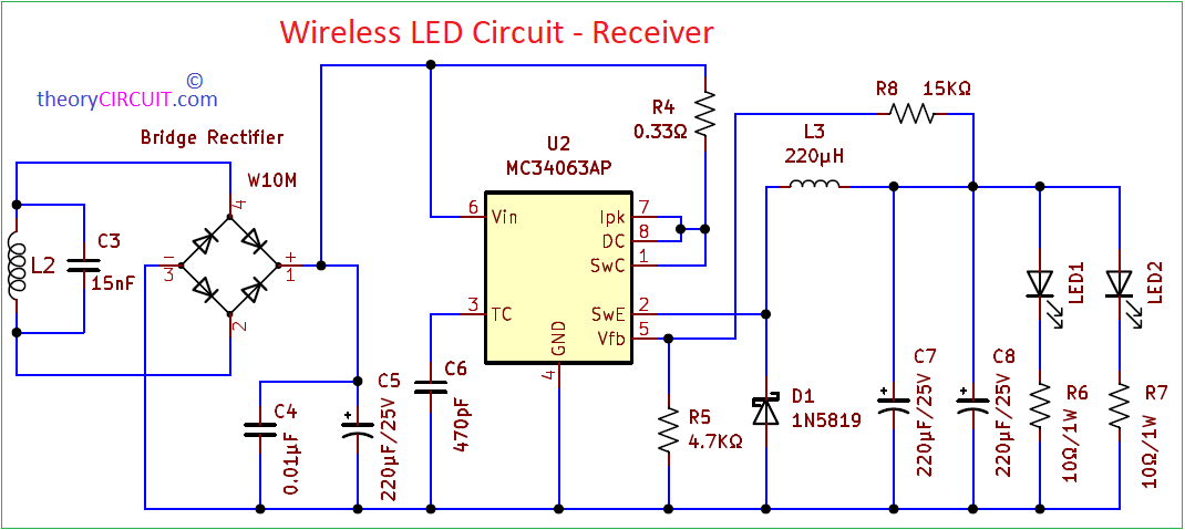
Wireless Power Receiver Circuit
Coil L2 Receives the fluctuating Electromagnetic Flux and Current flow induced, this alternating flow of current and voltage is fed into Bridge Rectifier module W10M, Rectified DC supply received from the positive and negative terminals. IC MC34063 is configured in boost converter mode and receives the DC supply.
In this configuration, the IC’s pins play important roles that is Pin 1 and Pin 2 connect to the external switch, Pin 3 is connected to the ground through 470pF Capacitor, Pin 4 is the ground reference, Pin 5 links to a resistor divider for feedback, Pin 6 is connected to positive supply, Pin 7 and Pin 8 connected with bias through R4. During start-up, the capacitor at Pin 3 charges, setting the oscillator frequency. The internal oscillator generates pulses, controlling the external switch (Pins 1 and 2) to facilitate energy storage in the inductor and subsequent release to the load, resulting in boosted output voltage. The feedback loop, involving Pin 5, ensures voltage regulation. External components, including an inductor, diode, and capacitor, play crucial roles in this process. Understanding and optimizing these parameters are vital for efficient boost converter. At the end two high bright LEDs are connected. You can use this circuit to power or charge any gadgets with low voltage and requirements.