
Last Updated on April 20, 2024
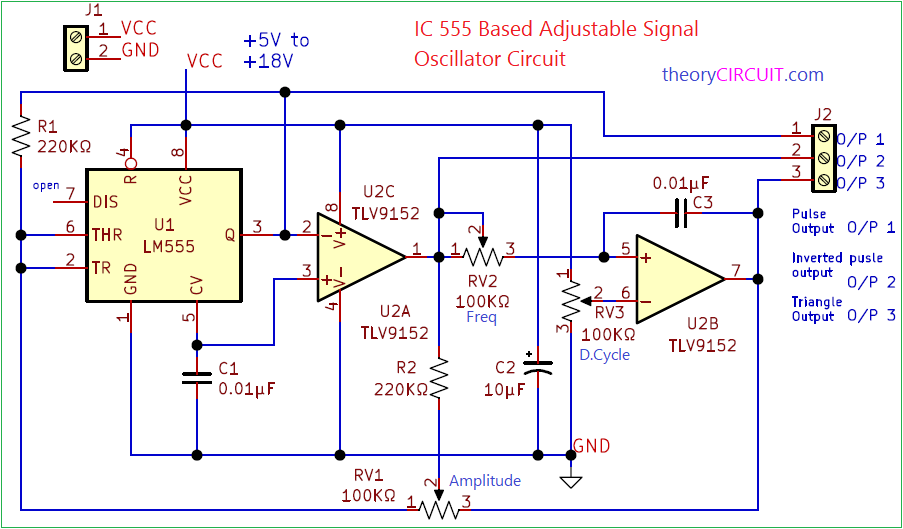
Oscillating Square pulse, Inverted square pulse and Triangle wave all together is not an difficult job when you employ Timer IC 555 with Dual, 16-V, 4.5-MHz, low-power operational amplifier IC TLV9152. This IC 555 Based Adjustable Signal Oscillator Circuit is cable of producing output waves with the control of Amplitude, Frequency and Duty cycle.
Timer IC LM555 from Texas Instruments is a highly stable device for generating accurate time delays or oscillation. Additional terminals are provided for triggering or resetting if desired. In the time delay mode of operation, the time is precisely controlled by one external resistor and capacitor called timing Resistor and timing capacitor.
IC TLV9152 from Texas Instruments is 4.5-MHz, Rail-to-Rail Input/Output, Low Offset Voltage, Low Noise general purpose operational amplifier. 8-Pin SOIC package contains two internal amplifiers (U2A and U2B) bias lines of the amplifier mentioned as U2C.
Circuit Diagram
Components Required
| 1 | C1, C3 | 0.01µF | C_1206_3216Metric | 2 | ||
| 2 | C2 | 10µF | C_Elec_4x5.4 | 1 | ||
| 3 | J1 | Screw_Terminal_01x02 | TerminalBlock_Altech_AK300-2_P5.00mm | 1 | ||
| 4 | J2 | Screw_Terminal_01x03 | TerminalBlock_Altech_AK300-3_P5.00mm | 1 | ||
| 5 | R1, R2 | 220KΩ | R_1206_3216Metric | 2 | ||
| 6 | RV1, RV2, RV3 | 100KΩ | Potentiometer_Bourns_3314J_Vertical | 3 | ||
| 7 | U1 | LM555 | SOIC-8_3.9×4.9mm_P1.27mm | 1 | ||
| 8 | U2 | TLV9152 | SOIC-8_3.9×4.9mm_P1.27mm | 1 |
Construction & Working
In this Signal Oscillator circuit IC LM555 configured as Square pulse generator with open discharge and IC TLV9152 U2B Amplifier makes positive feedback to the Timer IC555 and U2A Amplifier acts as a Inverting amplifier. Both U2A and U2B amplifiers are producing linear ramp slope signal. Variable Resistor RV1 takes responsibility to control output signal Amplitude. RV1 connects Output of U2B and Threshold, Trigger pins of U1. Variable terminal pin 2 of RV1 is connected with output of U2A through R2.
Frequency control of output signal is achieved through RV2 between U2A output and U2B Non inverting input. RV3 connected between C2 and inverting input pin of U2B amplifier makes difference in Duty cycle of output pulse. For three output signal you can use common ground supply. This circuit is designed to operate in the voltage between +5V to +18V / 500mA.
Printed Circuit Board
IC 555 Based Adjustable Signal Oscillator Circuit PCB Gerber files.

Interactive Board Viewer

