Last Updated on March 16, 2024
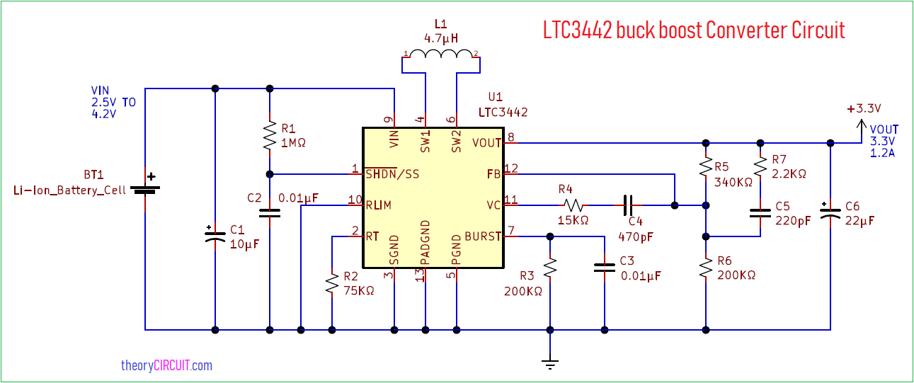
LTC3442 is Micropower Synchronous Buck-Boost DC/DC Converter Integrated Circuit with Automatic Burst Mode Operation and it can drive the output voltage and current above or below the input voltage and current, It has the input voltage range between 2.4V to 5.5V and output voltage range between 2.4V to 5.25V and this IC comes in small DFN package. Here LTC3442 Buck Boost Converter Circuit designed to give 3.3V at maximum current rating from li-ion battery input.
LTC3442 can be used in USB peripherals, low voltage medium current servos and handheld instruments, High power LED driver etc.., this circuit is suitable for SMD PCB fabrication.
Circuit Diagram
Components Required
- IC LTC3442
- Resistor 1MΩ, 75KΩ, 200KΩ=2, 15KΩ, 340KΩ, 2.2KΩ
- Capacitor 10µF, 0.01µF=2, 470pF, 220pF, 22µF
- Inductor 4.7µH
- 3.7V Li-ion battery
Construction & Working
Due to the IC LTC3442 DFN package this circuit can be done in SMD PCB and for this prototype we have used 0805 (imperial code) size SMD components, This circuit maintains the output at 3.3V and it may above or below the input voltage.
The internal error amp output voltage on VC determines the output duty cycle of the switches. The IC LTC3442 provides four different automatic operations and gives high efficiency output. This buck boost converter IC utilize <1μA Shutdown Current only and for Quiescent 35 μA, Operating frequency and average input current limit can each be programmed with an external resistor. Additional features of LTC3442 is programmable soft-start, peak current limit and thermal shutdown.