Last Updated on March 16, 2024
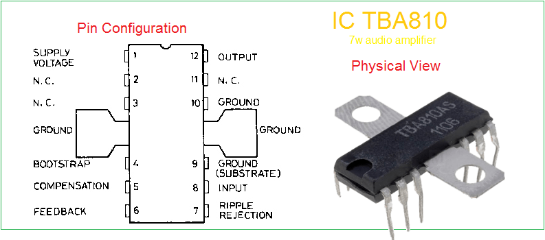
Simple and cost effective Audio Amplifier circuit diagram designed by using IC TBA810, it is a 7 watt audio amplifier Integrated circuit. It is fabricated as monolithic integrated circuit in a 12 lead quad in-line plastic package, intended for use as a low frequency class B amplifier, it is most suitable for general purpose low power audio amplifier design.
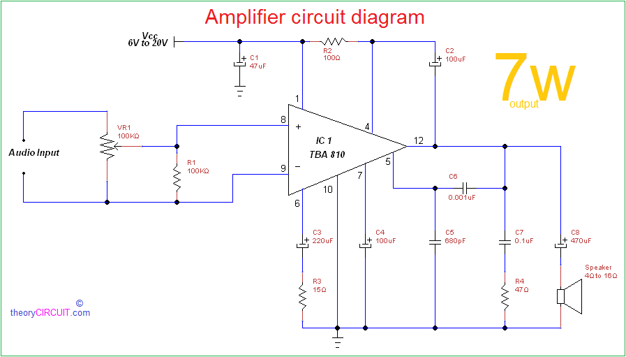
TBA 810 IC requires few RC components to give 7W output and this IC able to handle 6V to 20V (500mA) bias input and drives 4Ω to 16Ω speaker at output.
Circuit diagram
Construction & Working
Audio signal input given to the non inverting pin 8 of TBA 810 IC through volume control variable resistor VR1 and output is taken out from pin 12 and other pins are filled up with Resistor and capacitor components.
Tabs both side in IC are grounded and IC can be covered with heat sink, After completing the construction of circuit choose power supply depends on required output power.
Thus this circuit gives 1 watt output for 4 to 6V and 7 watt output for 16V bias, and it produce better output from 40Hz to 20KHz (-3dB) frequency input.
IC 810 Pin details