
Last Updated on March 24, 2024
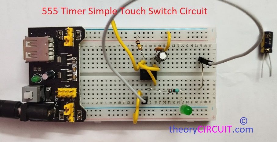
Even after 50 years of invention the Timer IC 555 is still rocking and here is the simple and easy to construct hobby or very useful circuit to control output with one touch. 555 Timer Simple Touch Switch Circuit is designed and tested with different timing capacitor and here we used a Green LED to indicate the output, you can use any kind of output actuators to control with one touch.
Here Timer IC 555 configured in Monostable multivibrator mode and trigger input pin 2 is connected with either small Copper strip or wire without insulation to give trigger signal by touching it. In this touch switch circuit IC 555 gives LOW output when there is no trigger signal applied, and gives HIGH output depends on the timing elements range when touching (triggering) occurs. After the output time duration IC 555 goes to LOW output stage. Here Green LED glows for HIGH and stays Off for LOW.
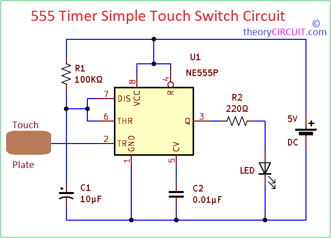
Circuit Diagram
Components List
- Timer IC NE555P
- LED
- Resistors 100KΩ, 220Ω each one
- Capacitors 10μF, 0.01μF each one
- Touch plate (Copper strip or wire without insulation)
- DC power supply
Construction & Working
In Monostable mode IC 555 Triggering Input Pin 2 is taken for external input (here touch plate or wire), Reset pin is connected with VCC, The Timing Resistor R1 is connected between Discharge, Threshold pin and Timing Capacitor C1. These two elements decides how much time duration? for output state HIGH. Use this calculator To calculate Monostable Multivibrator output time duration.
When the trigger input (touch) received lower than 1/3 of VCC, it triggers the Timer IC 555 internal flip flop. This causes the output (pin 3) to switch from a stable LOW state to a HIGH state. When trigger occurs internal discharge transistor is turned off and allowing the capacitor C1 to start charging through an external resistor R1. Time duration of capacitor C1 to charge to 2/3 of VCC is determined by the values of both external resistor R1 and capacitor C1. Once the capacitor C1 voltage reaches 2/3 of VCC, the threshold pin detects by internal comparator and causing the flip flop to reset that is output at pin 3 to return to its stable LOW state. Then discharge transistor is turned back ON and discharging the capacitor to ground through pin 7. This cycle repeats when ever we touch the trigger input.
Output pulse width duration can be calculated as T= 1.1 × R × C.
For an example if we use 10μF Capacitor as C1 in the above circuit,
Output pulse width duration T= 1.1 × 100000 Ω× 0.00001 F. => T = 1.1 Seconds.
For an example if we use 220μF Capacitor as C1 in the above circuit,
Output pulse width duration T= 1.1 × 100000 Ω× 0.00022 F. => T = 24.2 Seconds.