Last Updated on November 22, 2026
As you know Battery powered application likes buck converter Regulator rather than LDO (low dropout) Regulators. Because the LDO regulators drop voltage by burning excess power as heat. But the Buck converter switches output to regulate it. Here the simple 555 timer Buck Regulator circuit lets you reduce a 12 DC supply to any average voltage between 3V to 11.5V just by turning one potentiometer. This circuit uses only one LM555 timer IC, one IRF540N power MOSFET, and few components to act as timing element. So that you can build this circuit under 30 minutes.
Note that this circuit is designed to have minimum components as possible so that the output voltage may little pulsated like PWM DC chopper. If you want smooth DC for sensitive circuits then use proper filter components.
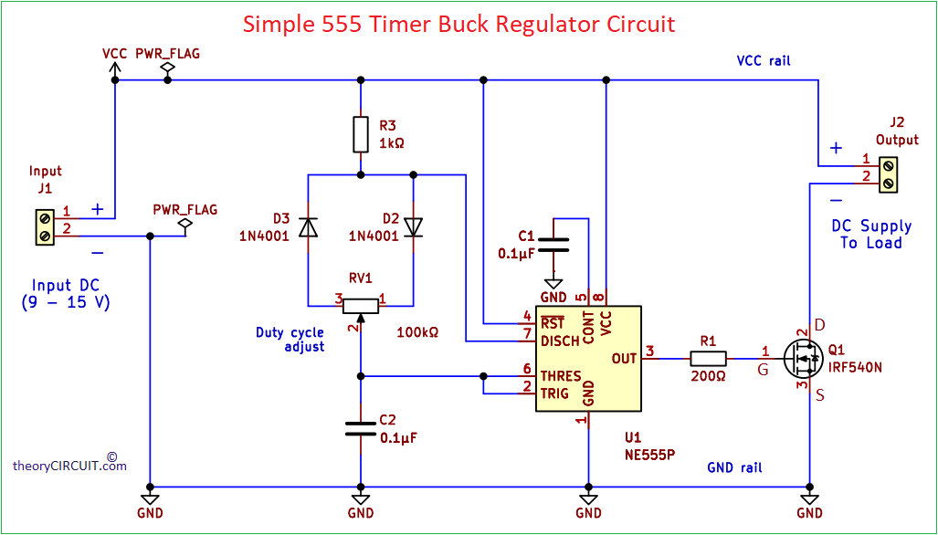
Circuit Diagram
Components Required
| 1 | C1 | 0.1µF | C_Disc_D5.0mm_W2.5mm_P5.00mm | 1 | ||
| 2 | C2 | 1nF | C_Disc_D5.0mm_W2.5mm_P5.00mm | 1 | ||
| 3 | R1 | 200Ω | R_Axial_DIN0207_L6.3mm_D2.5mm_P10.16mm_Horizontal | 1 | ||
| 4 | R3 | 1kΩ | R_Axial_DIN0207_L6.3mm_D2.5mm_P10.16mm_Horizontal | 1 | ||
| 5 | D2, D3 | 1N4001 | D_DO-41_SOD81_P10.16mm_Horizontal | 2 | ||
| 6 | U1 | NE555P | DIP-8_W7.62mm | 1 | ||
| 7 | Q1 | IRF540N | TO-220-3_Vertical | 1 | ||
| 8 | RV1 | 100kΩ | Potentiometer_Bourns_3386P_Vertical | 1 | ||
| 9 | J1 | Input | TerminalBlock_bornier-2_P5.08mm | 1 | ||
| 10 | J2 | Output | TerminalBlock_bornier-2_P5.08mm | 1 |
Working Video
Construction & Working
Here the 555 timer works as a PWM (Pulse Width Modulation) generator running range from few hundred Hz to 14 KHz. So the output pulses from 555 timer switches the IRF540N MOSFET ON and OFF very fast. When the MOSFET is ON then the load gets the full supply voltage, when it is OFF then the load gets nothing, by changing how long the MOSFET stays ON in each cycle (that is duty cycle), we can change the average power delivered to the load.
Printed Circuit Board
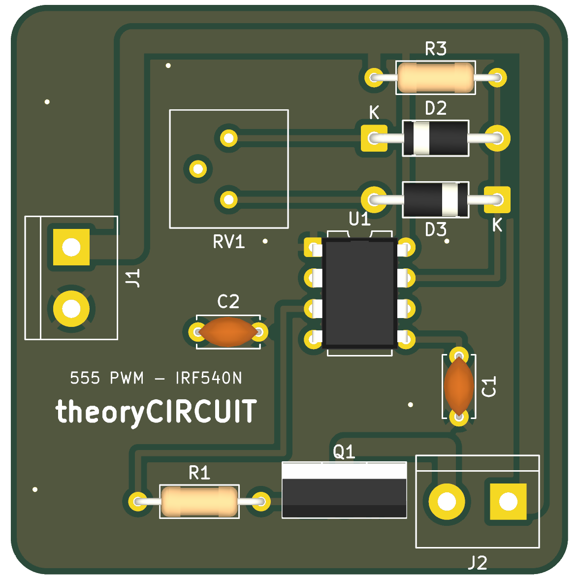
Interactive Board Viewer


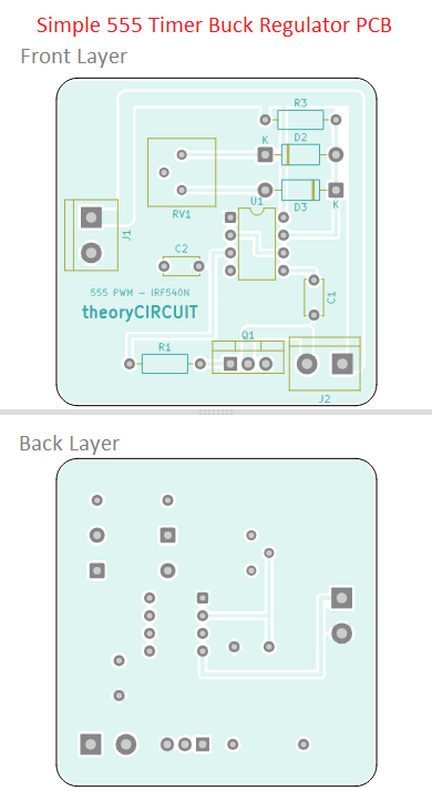
PCB Layers
Here the Whole circuit works on one simple idea that is switch the supply ON and OFF very fast and control the ON time. Here the 555 timer decides ON time and the MOSFET does the heavy current switching.
In this 555 buck regulator circuit timer IC 555 runs in astable mode (use Astable Multivibrator Calculator to identify output frequency and duty cycle). Pin 2 (trigger) and Pin 6 (Threshold) are connected together to the timing capacitor C2 and inside the 555 IC there are two comparators referenced at 1/3 Vcc and 2/3 Vcc. When the C2 voltage falls below 1/3 Vcc level then the output pin 3 goes HIGH and the discharge pin 7 turns OFF.
Then the C2 Voltage rises above 2/3 Vcc, then the output pin 3 goes LOW and pin 7 turns ON to short to ground. So that C2 keeps charging and discharging between 4V and 8V (at 12V supply) and the output keeps toggling.
Here the charging path is,
+VCC -> R3 (1KΩ) -> D2 -> RV1 -> C2
and the discharging path is
C2 -> RV1 -> D3 -> pin 7 -> GND
and this circuit average output voltage simply calculated as,
Vavg = Duty cycle x Vcc
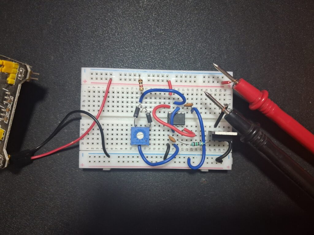
After constructing the circuit use multimeter or voltmeter to test the circuit by adjusting variable resistor RV1.
Simple 555 timer Buck Regulator Circuit Gerber Files
Gerber Files for 555 timer Buck Regulator circuit.
On Breadboard – Testing