Last Updated on March 16, 2024
Inverter circuit gives Alternating Current (AC) output from battery Power source, but the battery requires constant DC supply to get charge, so the every inverter circuit contains Rectifier and battery charger segment. We need to provide AC input power to those circuits, then only we can get AC output from inverter circuit.
When there is no AC supply outlet, we couldn’t charge the inverter battery & get high voltage output. In this article Photovoltaic solar based inverter circuit given with easily available components and it helps us to charge the inverter battery with out external AC supply outlet. It can be Encapsulated as handheld inverter.
Stages of PV solar power inverter
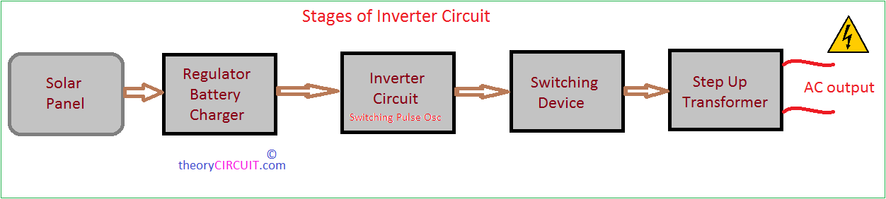
Photovoltaic solar inverter circuit constructed with five different stages.
- PV Solar panel
- Regulator / Battery chagerg
- Inverter Circuit (Switching Pulse Oscillator)
- Switching Device
- Step Up transformer (Output stage)
pv Solar inverter Circuit Diagram

Construction & Working
PV Solar Panel

In this circuit 12 Volt / 20 Watts Solar panel used to get input bias, It gives peak 12 volt at 1600 mA when exposed to the open Sun.
Regulator / Battery Charger
The LM317 adjustable three terminal Positive voltage Regulator used here and it can give output voltage range from 1.25 V to 37 V with more than 1.5A current rating. final output from the regulator is given to 12/4.5Ah SLA Battery, this Battery provides DC bias to the inverter circuit. Regulator LM317 output voltage Vout can be obtained as
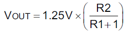
R2 => R2+VR1 for given inverter circuit.
Inverter Circuit using IC CD4047 (Switching Pulse Oscillator)
Monostable / Astable multivibrator IC CD4047 used here to produce switching pulse, This IC works in low power and available in 14 pin Dual in line package. It provides full Oscillation output F at Pin 13, 1/2 of oscillation at Pin 10 as Q and Pin 11 as Q’. each output pin gives 50% duty cycle.
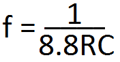
Here R => R4+VR2 and C=> C3. by using this formula we can obtain frequency output at pin 13. For pin 10 and 11 the formula changes as f=1/4.4RC.
MosFET drivers
IRF540 N Channel power mosfet from vishay siliconix used as a switching drivers for this inverter circuit. It gives fast switching, and have high operating temperature characteristics (175ºC).
Output Stage
Main part of solar iverter is output stage, here transformer X1 is used in reverse with specifications as 230V primary, 9V-0-9V / 1.5A secondary winding center tapped transformer. MOV (Metal oxide Varistor) protects electronic device connected at output.
Solar panel output voltage is directly fed into LM317 positive Regulator circuit and it is adjusted to give 12 volt output and Battery connected to this bias through (3A, 50V) Schottky diode.
The CD4047 IC is connected and configured as Astable multivibrator, When we turn ON SPST switch this circuit starts oscillation. Output Q and Q’ are directly fed into switching power mosfet IRF540 & drives X1 transformer secondary winding, here the current flow occurs particular duration and not for particular duration. So varying electromagnet induced and primary winding coil produce EMF, hence we get Alternating current output. Depends on the count of winding and switching frequency output Voltage/Frequency get varied.
Very interesting and Powerful
have you tried?
Have you tried implementing this?
i have tried the circuit ,it is not to be used for electronics ckts. o/p vol. and frequency varies with varying load and input voltage. o/p voltages shoots more than 300 v.! no regulation in o/p voltage.
have you tried?
nice.. is that ok for major project ? reply asap
is this works please provide solution asap