
Last Updated on March 16, 2024
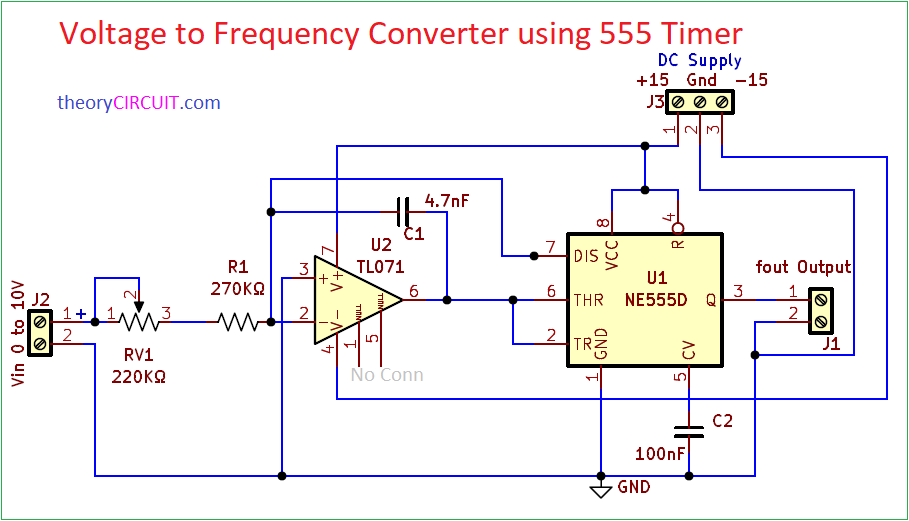
As we know A Voltage to Frequency Converter or VFC is an electronic circuit that converts an DC input voltage to a specific frequency square pulse signal. Voltage to Frequency Converter using 555 Timer transforms voltage variations into frequency variations. Frequency oscillation can be tuned by changing timing element. This type of circuit is widely used in various applications, especially in analog to digital converters and frequency modulation. The basic idea behind a VFC is to generate a frequency that is linearly proportional to the input voltage. This circuit takes 0V to 10V DC as input voltage. This circuit contains operational amplifier stage and Timer 555 Oscillator stage. The output frequency, usually in hertz (Hz) to Kilo hertz (KHz), corresponds directly to the input voltage.
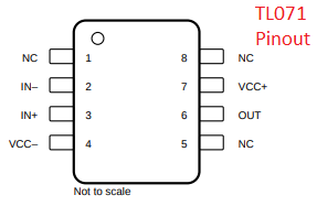
IC TL071 is a JFET input operational amplifier with features including low offset (1 mV, typical), high slew rate (20 V/µs), and common-mode input to the positive supply. High ESD (1.5 kV, HBM), integrated EMI and RF filters, and operation across the full –40°C to 125°C. TL071 can be operated with 4.5V to 30V DC Supply input.
| Pin Num, Name | Pin Description |
| 1, NC | No Connection pin Do not connect |
| 2, IN- | Operational Amplifier Inverting Input Pin |
| 3, IN+ | Operational Amplifier Non Inverting Input Pin |
| 4, VCC- | Power Supply Negative |
| 5, NC | No Connection pin Do not connect |
| 6, OUT | Operational Amplifier Output Pin |
| 7, VCC+ | Power Supply Positive |
| 8, NC | No Connection pin Do not connect |
Circuit Diagram
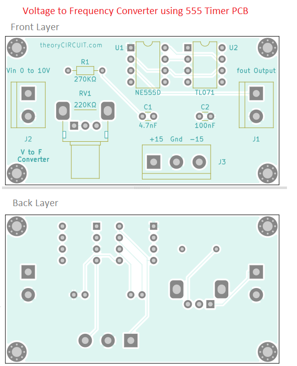
Components Required (BOM for PCB)
| 1 | C1 | 4.7nF | C_Disc_D3.0mm_W1.6mm_P2.50mm | 1 | ||
| 2 | C2 | 100nF | C_Disc_D3.0mm_W1.6mm_P2.50mm | 1 | ||
| 3 | R1 | 270KΩ | R_Axial_DIN0204_L3.6mm_D1.6mm_P7.62mm_Horizontal | 1 | ||
| 4 | U1 | NE555D | DIP-8_W7.62mm | 1 | ||
| 5 | U2 | TL071 | DIP-8_W7.62mm | 1 | ||
| 6 | RV1 | 220KΩ | Potentiometer_Alps_RK09K_Single_Horizontal | 1 | ||
| 7 | J1 | fout Output | TerminalBlock_bornier-2_P5.08mm | 1 | ||
| 8 | J2 | Vin 0 to 10V | TerminalBlock_bornier-2_P5.08mm | 1 | ||
| 9 | J3 | +15 Gnd -15 | TerminalBlock_bornier-3_P5.08mm | 1 |
Construction & Working
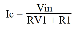
This V to F converter circuit uses operational amplifier TL071 as input trigger amplifier to the timer IC and IC 555 as Astable Multivibrator. This Circuit takes 0 to 10 Volt DC as input signal, and gives output square pulse with frequency range 0 to 1000 Hz. C1 capacitor acts as a feedback to the operational amplifier and the current flow through this element can be calculated as follows.
When the voltage level on the C1 reaches the 2/3 of timer IC 555 then internal discharge transistor of 555 gets open, hence voltage on C1 comes to 1/3 the voltage of VCC and this is lower comparator threshold of timer IC 555. At this level the discharge transistor switches off then C1 starts charging again. The Timer IC 555 output is HIGH while C1 Capacitor is charging and LOW while C1 capacitor is discharging. By this operation we can easily calculate the output frequency as

Here RV1 can be used to change output frequency and the input voltage. Output frequency will have less than 2% tolerance.
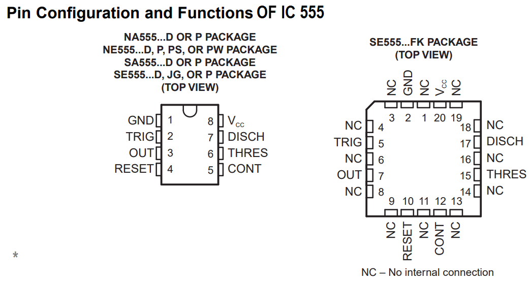
IC 555 Timer Pinout
Printed Circuit Board
Voltage to Frequency Converter using 555 Timer Gerber Files.
Interactive Board Viewer

