Last Updated on April 27, 2024
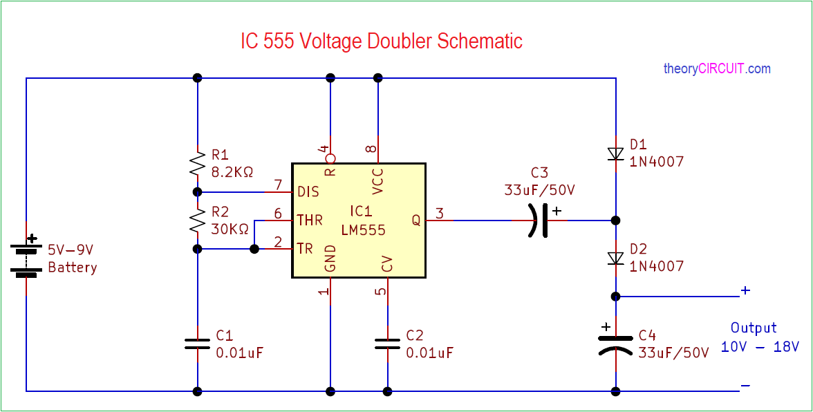
Simple and easy to construct IC 555 based voltage doubler schematic given here, This circuit will double the Input bias as 5V – 9V to 10V – 18V output. This circuit can be used as a charge bump or DC to DC boost converter, When our design includes Stepper motor or servo motors we can simply generate bias for those motors from this simple circuit. We don’t need separate power supply circuit.
This circuit delivers high frequency square pulse output and C3 capacitor holds the pulse charge and D2 diode Rectifies positive peak of square pulse and C4 gets the peak voltage charge and gives doubled output voltage combined with input bias through D1 diode.
IC 555 Voltage Doubler Circuit Diagram
Components Required
- IC 555
- Capacitors 33μF/50V = 2
- Capacitors 0.01μF = 2
- Diode 1N4007 = 2
- Resistor 8.2KΩ, 30KΩ each one
- 9V Battery
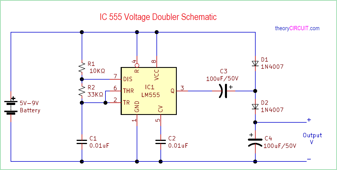
Another IC 555 Voltage Booster Circuit
Working Video
Construction & Working
Simple IC 555 voltage doubler schematic constructed in the structure of Astable multivibrator, This circuit will provide output duration depends on timing Resistor R1, R2 and timing Capacitor C1.
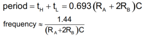
Here, RA = R1, RB = R2, and C = C1.
You Can use this IC 555 Astable Multivibrator Calculator for to know exact frequency output.
By changing these timing components we can obtain different level of output, but very low frequency or very high frequency output from timer won’t give best output voltage.
This circuit don’t have any over current draw protection setup and the load current output is slightly unstable hence it is suitable for low current applications only.
what will be the percentage out put current from doubling of voltage.
Dear Nagaraja,
two points to mention. First, the output voltage will be, at BEST, 2x diode voltage (= 2×0.7=1.4V) lower as the ideal theory gives. Second, on your question: the output current will be about twice the current drawn from the 555 output Q.