
Last Updated on July 12, 2025
Many Circuits are available online for PWM Signal generation but very few for external signal PWM and that too without testing and simulation. Here is the External Signal PWM Modulation Circuit using timer IC 555. Which can be useful for understanding the concept of PWM and modulation using external sine signal, pulse signal input.
What is PWM on field?
We can say straightly PWM is Pulse Width Modulation, that is pulse with fixed frequency and Variable Duty Cycle. Here the duty cycle is percentage of ON time in single pulse. For PWM signal, duty cycle varies according to the input either signal or voltage.
In practical applications, two different PWM signals are used, First one in circuits to Control Power Delivery to Motors, LED, Servo, Power supply regulation, Inverter etc.. we can name it as power electronics PWM! Secondly PWM signal in Communication like radio etc., Here message signal is modulated in the pulse width of carrier signal (Pulse input). Now we are going to simulate this kind of circuit using simple and easily available 555 IC.
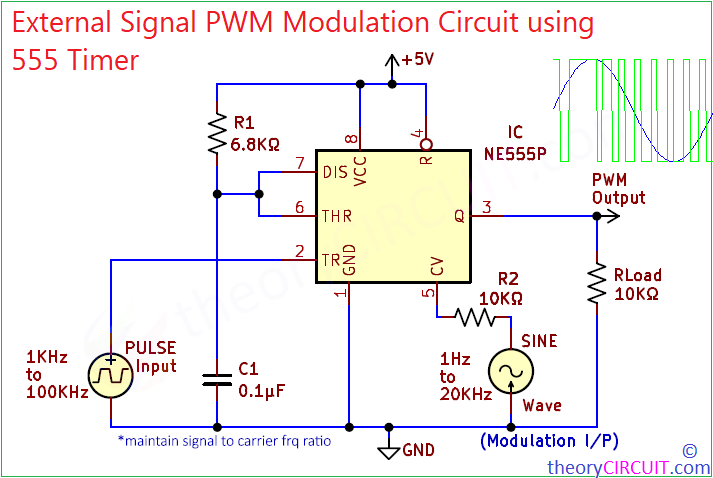
Circuit Diagram
Components Used
| Label | Component | Value/Type | Description / Note |
|---|---|---|---|
| IC | NE555 Timer IC | NE555P | Main PWM generator |
| R1 | Resistor | 6.8KΩ | Sets timing with C1 |
| R2 | Resistor | 10KΩ | Modulation control (signal input path) |
| RLoad | Resistor (or actual load) | 10KΩ | Represents connected output load |
| C1 | Capacitor | 0.1µF (100nF) | Timing capacitor |
| Pulse Input | Signal Generator | 1KHz to 100KHz Square Wave | Carrier frequency input |
| Sine Wave | Signal Generator | 1Hz to 20KHz Sine Wave | Modulating signal input |
| Power Supply | +5V | Can be 5V to 15V depending on IC version |
Construction & Working
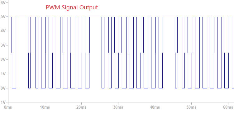
Here the PWM Oscillating element is timer IC 555, which is configured in Astable Multivibrator mode with fine adjustment that is Instead of timing Resistor between threshold pin and trigger pin we are going to use external signal which is a pulse input (Carrier signal). Then Sine signal as message (modulation input) is fed into control voltage pin. Always maintain signal to carrier frequency ratio that is carrier signal frequency and voltage should be higher than the message signal frequency and voltage.
In Astable Multivibrator mode IC 555 generates continuous square wave here depends on the trigger input from pulse input. The Duty cycle of output signal will be depend on control voltage pin input sine signal. 2/3 VCC is the threshold voltage and 1/3 VCC is the trigger voltage for this pin. This pin prevents the threshold comparator from being triggered when receives greater than 2/3 VCC and prevents trigger comparator from detecting falling edge when receives less than 1/3 VCC. By applying sine signal, the voltage to Pin 5 moves up and down which modifies the normal internal reference voltage,
Upper threshold = 2/3 VCC
Lower threshold = 1/3 VCC
This timing threshold shift dynamically based on input Sine wave to Control Voltage Pin 5.
It cause the output duty cycle to vary in real time and the frequency locked with carrier pulse input.
Refer Astable Multivibrator using 555 for more details about the calculation and internal operations.
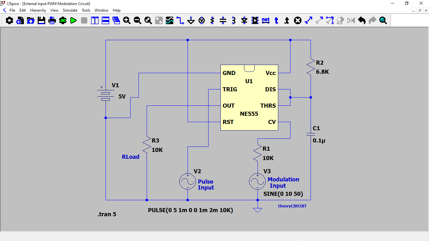
Simulation through LTSpice
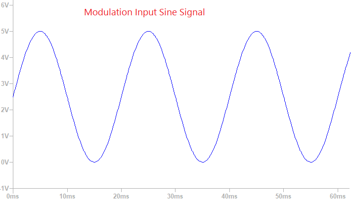
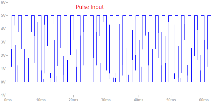
Waveforms
Lets check it with actual voice (mic input) next time.