
Last Updated on March 16, 2024
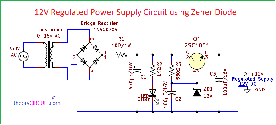
For any Electronic circuit a stable and Regulated power supply is essential for ensuring the proper functioning. There are several methods available to use but One simple, efficient and cost effective method of achieving this is by using a Zener diode, here 12V Regulated Power Supply Circuit using Zener Diode designed to give stable 12 Volt DC supply and this is configured as Transistor Series Voltage Regulator or Emitter Follower Voltage Regulator. Hence it is suitable for high current draw circuit applications.
In the following 12 Volt Zener regulator circuit, Transistor Q1 is Series pass transistor. Here Zener diode provides the reference voltage and Q1 acts as a variable Resistor and Resistance varies with the base current IB. In reverse bias Zener diode Conducts in Zener breakdown region. So the Output at the Emitter terminal will be,
Vout = Vz – VBE
Due to constant Voltage at the base of transistor, any voltage changes in the collector will not appear on the emitter terminal, hence we can obtain constant Regulated output supply.
Circuit Diagram
Components Required
| S.No | Designator | Value | Part Number | Quantity |
| 1 | TR1 | 230V to 0-15V AC | 0-15V Stepdown Transformer | 1 |
| 2 | C1 C2 | 470µF/16V 100µF/16V | Electrolytic capacitor Electrolytic capacitor | 1 2 |
| 3 | R1 R2 R3 | 10Ω/1W 1KΩ/0.5W 560Ω/0.5W | – – – | 1 1 1 |
| 4 | BR | Bridge Rectifier Module | Bridge Rectifier 1N4007 X 4 | 1 |
| 5 | LED1 | Green | – | 1 |
| 6 | ZD1 | 12V | Zener Diode | 1 |
| 7 | Q1 | 2SC1061 | NPN Transistor | 1 |
Construction & Working
Construction of this 12 Volt Regulated Power Supply Circuit using Zener Diode is very simple, first thing you need to bring at least 15V AC by using Stepdown transformer, then Convert this AC Supply into DC by using Bridge Rectifier module or Four 1N4007 diode bridge arrangement. Then This DC supply filtered by Capacitor C1 and LED indicates the presence of power supply. Resistor R3 and Capacitor C2 connected in series between positive and negative lines to provide VBC supply to transistor Q1. Value of R3 resistor have impact on Current flow to Base terminal of Q1 (IB). Transistor base terminal connected with reverse biased 12 Volt Zener diode. This ZD1 provides constant Voltage (Zener breakdown) at the transistor base and being responsible for regulated output voltage. By changing the Zener diode we can have different voltage level regulator.
2SC1061 Pinout
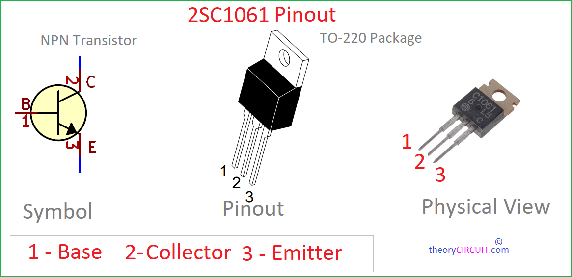
The 2SC1061 is a widely used NPN bipolar junction transistor (BJT) with a variety of applications in electronic circuits, this transistor is designed for general purpose amplifier application and switching application. With its low power dissipation and high current capability, the 2SC1061 is often employed in audio amplifiers, voltage regulators, and various signal processing circuits. Its typical collector current ranges from a few milliamperes to a maximum of 1.5 amperes, making it suitable for medium power applications. This transistor comes in a TO-220 plastic package, providing efficient heat dissipation and ease of handling during assembly.